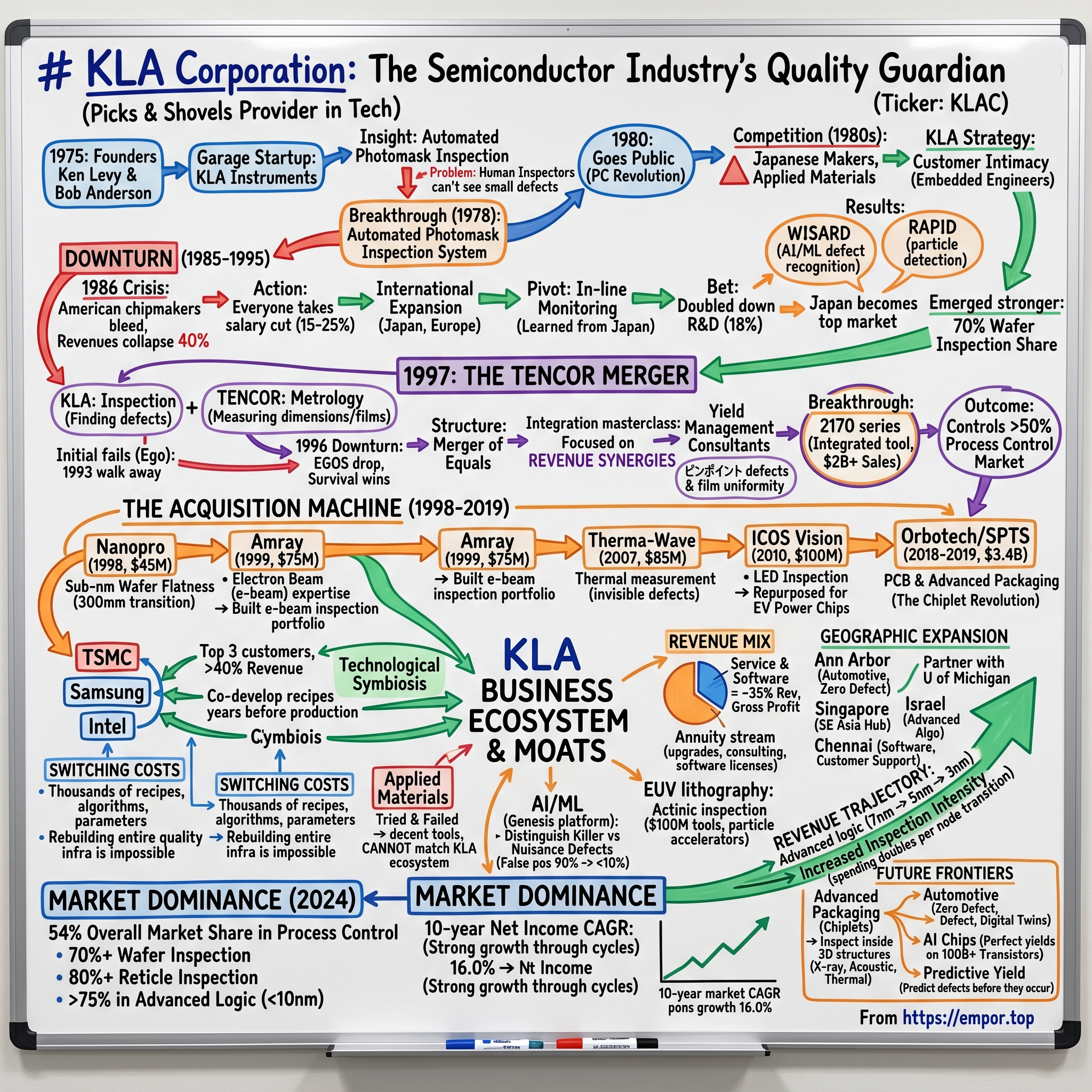
KLA Corporation: The Semiconductor Industry's Quality Guardian
I. Introduction & Episode Teaser
Picture this: Every smartphone in your pocket, every GPU powering ChatGPT, every chip in your Tesla—they all have something in common. Before they ever left the factory floor, they were scrutinized thousands of times by machines so precise they can detect defects smaller than a coronavirus particle. And there's a 70% chance those machines came from a company you've probably never heard of.
KLA Corporation commands the semiconductor inspection kingdom with the authority of a medieval gatekeeper—nothing passes through the silicon gates without their blessing. With a market cap hovering around $90 billion, they've built the most dominant franchise in semiconductor process control, wielding advanced inspection tools, metrology systems, and computational analytics that determine whether a chip lives or dies. They're the quality police of the semiconductor world, and their verdicts are final.
Here's the staggering part: KLA touches virtually every advanced chip manufactured on Earth. When TSMC needs to ensure their 3-nanometer process is yielding properly, they turn to KLA. When Samsung discovers mysterious defects killing their yields, KLA's machines hunt them down. When Intel lost their manufacturing edge in the 2010s, inadequate process control—the very thing KLA specializes in—was partly to blame.
This is the story of how two engineers named Ken and Bob built a garage startup in 1975 that would become the arbiter of semiconductor quality. It's a tale of surviving brutal industry cycles, executing a textbook merger of equals, and building an M&A machine that assembled the full stack of process control technology. Along the way, we'll discover why being the "picks and shovels" provider in semiconductors might be the best business model in all of technology.
The journey ahead takes us from Silicon Valley garages to Shanghai fabs, from optical microscopes to AI-powered defect detection, from a $60 million revenue business to an $8 billion juggernaut. We'll explore how KLA built moats so deep that even mighty Applied Materials can't cross them, why their 54% market share actually understates their dominance, and how they've managed to grow through every semiconductor downturn since Carter was president.
Buckle up—we're about to dive into the world of angstroms, yields, and the relentless pursuit of perfection that powers our digital age. This is the KLA story.
II. Founding Story & Early Silicon Valley Days (1975-1985)
Ken Levy was frustrated. It was 1975, and he'd spent years in aerospace simulation before landing at Computervision's Cobilt Division, where he watched semiconductor manufacturers struggle with a problem that seemed almost laughably basic: they couldn't see what was wrong with their chips. The inspection equipment of the era was primitive—essentially microscopes operated by humans peering at wafers for hours, a process about as reliable as finding needles in haystacks while wearing sunglasses.
Enter Bob Anderson, Computervision's CFO, a numbers guy with an unusual gift for spotting technical opportunity. When Levy pitched his vision for automated inspection systems that could combine advanced optics with high-speed digital electronics, Anderson didn't just write a check—he quit his job to co-found the company. Their partnership was instant chemistry: Levy the visionary technologist, Anderson the operational strategist. They would remain joined at the hip for the next 15 years, building what would become KLA Instruments.
The founding insight was deceptively simple yet technically audacious. While everyone else in 1975 was racing to make chips smaller and faster, Levy and Anderson realized that as geometries shrank, defects would become exponentially more catastrophic. A speck of dust that was irrelevant on a 10-micron process would be a chip-killer at 1 micron. They weren't building tools to make chips—they were building tools to save them.
Their secret weapon arrived in the form of Paul Sandland, an engineer's engineer who spoke fluent optics and electron beams. Sandland didn't just join KLA; he essentially built two parallel technology groups from scratch—one focused on optical inspection, another on electron beam technology. His teams worked 80-hour weeks in a Sunnyvale garage, hand-assembling systems that combined custom optics with proprietary software running on Digital Equipment Corporation minicomputers.
The breakthrough came in 1978 with their first commercial product: an automated photomask inspection system. Photomasks were the stencils used in lithography, and a single defect could ruin thousands of wafers. KLA's system could scan an entire mask in minutes, finding defects that human inspectors would miss after hours of searching. The semiconductor industry, desperate for yield improvements, snapped them up.
By 1980, just five years after founding, KLA went public. The timing was perfect—the semiconductor industry was exploding, driven by the personal computer revolution. Orders poured in from Intel, AMD, and Motorola. The company's revenues rocketed past $60 million by the mid-1980s, a 100x increase from their first year of sales. They dominated photomask inspection with 70% market share and were rapidly expanding into wafer inspection.
But success in Silicon Valley attracted competition like blood in the water attracts sharks. Japanese companies like Hitachi and Nikon, flush with cash from their domestic semiconductor boom, began developing competing systems. Applied Materials, already a giant in deposition equipment, started eyeing the inspection market. The easy years were ending.
KLA's response revealed the strategic DNA that would carry them through the next four decades. Instead of competing on price or features, they went all-in on customer intimacy. They embedded engineers at Intel and IBM, learning their processes so deeply that KLA's tools became extensions of their customers' manufacturing lines. They didn't just sell machines; they sold yield improvement, measured in basis points that translated to millions in additional revenue.
By 1985, KLA had established three critical competitive advantages that would prove durable for decades. First, their installed base created switching costs—customers had years of data, recipes, and trained operators tied to KLA systems. Second, their R&D intensity (spending over 15% of revenue while competitors spent 8-10%) kept them a generation ahead technologically. Third, and most importantly, they'd positioned themselves as mission-critical—when yields dropped, CEOs called KLA.
The stage was set for the company's first existential test. Little did Levy and Anderson know that their small inspection company would soon face a crisis that would destroy half of Silicon Valley's semiconductor equipment makers. The Japanese were coming, and they weren't taking prisoners.
III. Surviving the First Semiconductor Downturn (1985-1995)
The numbers were catastrophic. By 1986, Japanese semiconductor manufacturers had gone from virtually nothing to commanding 50% of global market share. American chip makers were bleeding—AMD laid off 15% of its workforce, National Semiconductor shut entire fabs, and even Intel, the industry's gold standard, posted its first loss as a public company. For equipment suppliers like KLA, it was an extinction-level event.
Ken Levy called an all-hands meeting in KLA's Sunnyvale headquarters. The cafeteria was silent as he delivered the news: revenues had collapsed 40% in six months, their biggest customers were canceling orders, and without drastic action, KLA had maybe eight months of cash left. Then came the ask: everyone, from engineers to executives, would take a 15% salary cut. Officers would take 25%. "We're either going to survive this together," Levy said, "or we're all going to be looking for jobs together."
The salary cuts bought time, but KLA needed a strategy beyond survival. While competitors retreated to their home markets, KLA did something counterintuitive—they doubled down on international expansion. By 1984, before the crisis hit, they'd already generated 22% of sales from Japan and Europe. Now, with American fabs shutting down, they deployed their best engineers to Tokyo and started learning how Japanese manufacturers achieved their legendary yields.
What they discovered changed everything. Japanese fabs weren't just cleaner or more disciplined—they were religious about in-line monitoring. While American manufacturers typically inspected wafers at the end of the process (when it was too late to fix problems), the Japanese checked constantly, catching defects before they compounded. KLA's existing tools were perfect for this approach; they just needed to adapt them for higher-volume, continuous inspection.
The pivot required massive R&D investments at the worst possible time. While cutting salaries and laying off 20% of their workforce, KLA somehow maintained R&D spending at 18% of revenue—nearly double the industry average. The bet paid off with two breakthrough products: WISARD (Wafer Inspection System with Automatic Defect Recognition) in 1988 and RAPID (Real-time Automatic Particle Inspection Device) in 1990.
WISARD was particularly revolutionary. Using pattern recognition algorithms that would later be called machine learning, it could distinguish between killer defects and harmless anomalies, reducing false positives by 90%. RAPID brought contamination detection directly into the clean room, catching particle problems before they ruined entire lots. Japanese customers, initially skeptical of American equipment, became KLA's biggest advocates.
The financial turnaround was dramatic. From a low of $45 million in 1987, revenues climbed to $161 million by 1990. More importantly, KLA emerged from the downturn with an even more dominant position—70% of the wafer inspection market and 80% of reticle inspection. Competitors like Optical Specialties and Inspex had either gone bankrupt or been acquired for pennies on the dollar.
But the real victory was strategic. KLA had learned to thrive in downturns by becoming even more essential to customers desperate to improve yields. They'd proven that process control wasn't a luxury in bad times—it was a necessity. When you're running fabs at 50% capacity, every chip matters more.
The company also discovered the power of geographic diversification. While U.S. sales remained depressed through 1991, Asian revenues exploded as Samsung, TSMC (founded in 1987), and other Asian players entered advanced manufacturing. KLA established subsidiaries in Korea, Taiwan, and Singapore, building relationships that would prove invaluable decades later.
Stock market investors initially didn't grasp the transformation. KLA's stock languished below $10 throughout the early 1990s, even as the company posted record profits. Wall Street saw semiconductor equipment as hopelessly cyclical, a feast-or-famine business unsuitable for serious investors. They missed the critical insight: KLA wasn't really selling equipment—they were selling insurance against yield loss.
By 1995, KLA had grown to 2,500 employees and was generating over $600 million in annual revenue. But Levy and Anderson knew they faced a new challenge. The industry was consolidating rapidly—Applied Materials had grown into a $3 billion behemoth through aggressive acquisitions, and Japanese giants like Tokyo Electron were expanding globally. KLA needed scale to compete in the next generation of 300mm wafers and sub-100nm processes.
The solution would come from an unexpected source: their mirror image across the San Francisco Bay. Tencor, founded the same year as KLA with a complementary technology portfolio, was having the exact same strategic conversation. What happened next would create the process control powerhouse that dominates the industry today.
IV. The Tencor Merger: Creating a Process Control Powerhouse (1997)
Karel Urbanek had a problem that sounded absurd to anyone outside the semiconductor industry: he needed to measure things that were literally invisible. It was 1976, just one year after KLA's founding, and Urbanek, a Czech immigrant with a PhD in physics, had discovered that chipmakers were flying blind when it came to film thickness. They'd deposit layers of materials just nanometers thick, but had no reliable way to verify the thickness until after the entire wafer was processed—by which time millions of dollars of product could be ruined.
Urbanek partnered with John Schwabacher, a venture capitalist who understood the physics and the business opportunity. Together they founded Tencor (TENcor = Thin-film ENCORe), building instruments that used ellipsometry and laser-scanning to measure film properties in real-time. While KLA was finding defects, Tencor was ensuring films were the right thickness—two sides of the same process control coin.
For fifteen years, KLA and Tencor circled each other like binary stars, occasionally competing but mostly operating in parallel universes. KLA owned inspection (finding particles and pattern defects), while Tencor dominated metrology (measuring critical dimensions and film properties). Their customers were identical—Intel, IBM, Texas Instruments—but their technologies were entirely complementary.
The first dance began in 1992. The semiconductor industry was in another cyclical trough, and both companies were burning cash to develop 300mm wafer tools. Investment bankers from Morgan Stanley arranged a dinner between the executive teams at a Palo Alto restaurant. The conversation was electric—every KLA weakness was a Tencor strength, and vice versa. They could eliminate duplicate R&D, combine sales forces, and offer customers a complete process control solution.
But the deal fell apart in 1993 over a painfully human issue: who would run the combined company? Ken Levy insisted on remaining CEO, while Tencor's team believed their stronger financial performance (higher margins despite lower revenues) warranted equal representation. After six months of negotiations, they walked away, each convinced they could win alone.
The 1996 semiconductor downturn changed everything. Memory prices collapsed 80%, dragging equipment spending down with them. Both companies saw orders evaporate overnight. KLA's stock fell from $45 to $18; Tencor dropped from $32 to $14. This time, when the bankers suggested meeting again, ego took a backseat to survival.
The second negotiation was different. Ken Levy, now 61 and thinking about succession, agreed to become Chairman while Tencor's CEO Ken Schroeder would run the combined company. They structured it as a merger of equals—a one-to-one stock swap valuing the combined entity at $1.3 billion. KLA brought 2,500 employees and $600 million in revenue; Tencor contributed 1,400 employees and $403 million in revenue.
Wall Street's reaction was unprecedented for a semiconductor equipment merger: universal acclaim. Analysts called it "the most complementary merger in semiconductor history." The combined company would control over 50% of the process control market, with virtually no product overlap. Goldman Sachs upgraded the stock immediately, noting that customers had been begging for integrated inspection and metrology solutions for years.
The integration, announced in 1997, was a masterclass in merger execution. Instead of the typical cost-cutting bloodbath, KLA-Tencor focused on revenue synergies. They created "yield management consultants" who could diagnose problems using both inspection and metrology data—something neither company could do alone. When Intel's yields dropped on a new process, KLA-Tencor engineers could pinpoint whether the issue was particles (inspection) or film uniformity (metrology) and prescribe solutions.
The financial results were staggering. Combined revenues hit $1.2 billion in 1997, but more importantly, operating margins expanded from 15% to 23% within two years. The company didn't just add revenues—it multiplied value. Customers who previously bought inspection tools from KLA and metrology from Tencor now bought integrated solutions at premium prices.
The merger also created unexpected technological synergies. KLA's expertise in high-speed image processing combined with Tencor's precision measurement algorithms produced a new generation of tools that could do both inspection and metrology in a single pass. The 2170 series, launched in 1999, became the highest-revenue product in semiconductor equipment history, generating over $2 billion in sales.
But the real genius of the merger was strategic positioning. As chip geometries shrank below 180nm, the line between inspection and metrology blurred. A particle might actually be a malformed feature; a dimension might be wrong because of contamination. KLA-Tencor's integrated approach meant they could solve problems competitors couldn't even diagnose.
By 2000, just three years post-merger, KLA-Tencor's market cap had grown from $1.3 billion to over $15 billion. They controlled 70% of wafer inspection, 80% of reticle inspection, and 60% of metrology. Competition from Applied Materials and Hitachi had been effectively neutralized—they simply couldn't match the breadth of KLA-Tencor's portfolio.
The merger set a template that KLA-Tencor would follow for the next two decades: find complementary technologies, integrate them deeply, and create solutions that customers couldn't get anywhere else. The acquisition machine was just getting started.
V. The Acquisition Machine: Building the Full Stack (1998-2019)
Ken Schroeder had a thesis that would transform KLA-Tencor from a merger success story into an acquisition juggernaut: process control was evolving from hardware to software, from detection to prediction, from tools to solutions. Standing before the board in 1998, barely a year after the Tencor merger closed, he laid out an audacious plan—acquire every critical piece of process control technology before competitors realized their value.
The shopping spree began immediately with Nanopro GmbH, a small German company with 30 employees and $8 million in revenue. To outsiders, paying $45 million seemed insane—a 5.6x revenue multiple for a niche interferometric measurement tool. But Schroeder saw what others missed: Nanopro's technology could measure wafer flatness to sub-nanometer precision, critical for the coming transition to 300mm wafers. Within three years, every advanced fab needed this capability, and KLA-Tencor owned the only solution.
Next came Amray Inc., acquired for $75 million, bringing scanning electron microscope (SEM) technology in-house. The genius wasn't the microscopes themselves—it was the electron beam expertise that KLA-Tencor could apply across their entire portfolio. They recruited Amray's top physicists to develop e-beam inspection tools that could find defects invisible to optical systems. By 2001, e-beam inspection revenues exceeded the entire Amray acquisition price.
The 2000 dot-com crash created unexpected opportunities. While competitors conserved cash, KLA-Tencor went hunting. Revenue grew 40% and net profit surged 74% in 2001—a year when most semiconductor companies posted losses. This cash generation funded a series of strategic acquisitions that would define the company's next decade.
The crown jewel came in 2007: Therma-Wave, acquired for $85 million. Therma-Wave had developed thermal measurement technology that could detect invisible defects by measuring heat dissipation patterns. More importantly, they'd cracked the code on measuring multi-layer film stacks—essential for advanced memory devices. KLA-Tencor integrated Therma-Wave's algorithms into their existing tools, creating a metrology platform that could measure things competitors couldn't even detect.
But the acquisition strategy wasn't just about technology—it was about timing markets. In 2010, Schroeder's successor Rick Wallace noticed LED manufacturers struggling with yield issues. He acquired ICOS Vision Systems for $100 million, gaining LED inspection tools just as solid-state lighting exploded. When the LED market cooled, they repurposed the technology for power semiconductors used in electric vehicles. Same tools, new market, 3x the revenue.
The boldest move came in 2018-2019 with the $3.4 billion acquisition of Orbotech, including its subsidiary SPTS Technologies. Orbotech dominated printed circuit board (PCB) inspection, while SPTS led in advanced packaging equipment. Wall Street was skeptical—why would a front-end semiconductor company buy back-end packaging tools? Wallace's answer was prescient: "The future of Moore's Law is advanced packaging. We're buying the future."
The Orbotech deal perfectly timed the chiplet revolution. As monolithic chips hit physical limits, the industry pivoted to advanced packaging—connecting multiple smaller chips to create powerful systems. Suddenly, KLA owned the inspection and metrology tools for both chip manufacturing and chip packaging, controlling quality across the entire semiconductor value chain.
Through these acquisitions, KLA-Tencor built capabilities that would have taken decades to develop organically. They acquired algorithms for AI-powered defect classification, simulation software for predicting yield, and data analytics platforms that could correlate defects across thousands of process steps. Each acquisition was a puzzle piece in a larger picture—the full stack of process control.
The financial discipline was remarkable. Despite spending over $5 billion on acquisitions between 1998 and 2019, KLA-Tencor maintained industry-leading margins and returned billions to shareholders through dividends and buybacks. They had a simple rule: acquisitions must be accretive to earnings within 12 months or they walked away. This discipline killed several high-profile deals, including a rumored $2 billion bid for Rudolph Technologies in 2015.
In 2019, the company made a subtle but significant change: dropping "Tencor" to become simply KLA Corporation. The rebrand reflected a transformation from two merged companies to a unified process control platform. With revenues approaching $6 billion and a market cap over $50 billion, KLA had assembled the most complete portfolio in process control history.
The acquisition machine had created something unprecedented: a company that touched every critical step in semiconductor manufacturing. From photomask inspection to wafer defect detection, from film measurement to advanced packaging, KLA owned the tools that determined whether chips worked or became expensive silicon coasters. The moat wasn't just wide—it was a maze that competitors couldn't navigate.
VI. Market Dominance & Competitive Positioning (2000-Present)
The numbers tell a story of dominance so complete it borders on monopolistic: 54% overall market share in process control, 70% in wafer inspection, 80% in reticle inspection. But Rick Wallace, CEO since 2006, knew these statistics actually understated KLA's true market position. Speaking to investors in 2020, he revealed the real number that mattered: "In advanced logic below 10 nanometers, our share exceeds 75%. We don't just lead the market—we define it."
The moat begins with switching costs that would make enterprise software companies jealous. When TSMC runs a 3-nanometer process, they're not just using KLA tools—they're running thousands of recipes, algorithms, and parameters developed over years of collaboration. A single fab might have 50 KLA tools generating terabytes of data daily, all integrated into yield management systems that took millions of engineering hours to optimize. Switching to a competitor wouldn't just mean buying new tools—it would mean rebuilding their entire quality infrastructure.
Applied Materials, the $150 billion gorilla of semiconductor equipment, has tried repeatedly to crack KLA's fortress. In 2003, they acquired Opal for $400 million to enter optical inspection. By 2008, they'd shut it down. In 2011, they bought Vistec for e-beam inspection. Market share peaked at 8% before declining. The pattern was always the same: Applied could build decent tools, but couldn't match KLA's ecosystem of software, service, and accumulated expertise.
The customer concentration that terrifies Wall Street analysts is actually KLA's greatest strategic advantage. Three customers—TSMC, Samsung, and Intel—represent over 40% of revenue. But this concentration creates intimate partnerships that transcend vendor relationships. When TSMC develops a new process node, KLA engineers are embedded two years before production, co-developing inspection recipes that become part of the process itself. It's not vendor lock-in—it's technological symbiosis.
The 2024 fiscal year showcased this dominance: $8.09 billion in revenue with 60% gross margins, a combination that shouldn't exist in capital equipment. For context, even mighty ASML, with their EUV monopoly, posts similar gross margins. KLA achieves this through a brilliant business model evolution—software and services now represent 35% of revenue but over 50% of gross profit. Every tool sold creates an annuity stream of upgrades, consulting, and software licenses that can exceed the original purchase price.
The competitive dynamics shifted dramatically during the AI boom of 2023-2024. As Nvidia's chips pushed the boundaries of reticle size and layer count, defect density requirements tightened by an order of magnitude. KLA's newest systems could find defects measuring 10 nanometers on chips with features measuring 3 nanometers—like finding a specific grain of sand on a beach from satellite imagery. Competitors simply couldn't match this sensitivity without years of algorithm development.
Market share tells only part of the story. In the most critical applications—EUV mask inspection, advanced logic yield management, 3D NAND metrology—KLA often has 90%+ share. These aren't just the highest-volume markets; they're the highest-value, where customers will pay millions for even a 0.1% yield improvement. A single EUV mask inspection tool costs $50 million, and every EUV fab needs multiple systems.
The cyclicality that plagued semiconductor equipment for decades has become manageable for KLA. During the 2023 downturn, while competitors saw revenues drop 20-30%, KLA declined just 8%. The installed base of over 50,000 systems worldwide generates steady service revenue, while the shift to more complex chips means inspection intensity (inspection spending per wafer start) continues growing even when wafer starts decline.
Tokyo Electron and Lam Research, formidable competitors in deposition and etch, have occasionally probed process control. But they face an impossible catch-22: to compete with KLA requires massive R&D investment, but without KLA's market share, they can't justify the spending. KLA spends $1.5 billion annually on R&D—more than most competitors' total profits.
The China factor adds complexity. Chinese customers represented 30% of revenue in 2023, but U.S. export controls increasingly restrict advanced tool sales. KLA's response has been surgical—maintaining older technology sales to China while ensuring their most advanced tools remain exclusive to allied nations. It's a delicate balance that requires constant navigation of geopolitical currents.
By 2024, with a market cap reaching $89.5 billion, KLA had become the third most valuable semiconductor equipment company globally, trailing only ASML and Applied Materials. But in process control—their kingdom—they reign supreme. As one industry veteran noted: "You can build chips without Applied Materials tools, you can even build them without ASML. But you can't build them profitably without KLA."
VII. Technology Evolution & Innovation Engine
The clean room at KLA's Milpitas technology center looks like something from science fiction—engineers in full bunny suits operating machines that cost more than private jets, hunting for defects smaller than DNA strands. But the real innovation happens in a nondescript building next door, where 500 PhDs in physics, mathematics, and computer science are solving problems that won't matter to customers for five years. This is KLA's innovation engine, consuming 55% of operating expenses—a ratio that would bankrupt most hardware companies but has become KLA's greatest competitive weapon.
The evolution from optical to electron beam inspection reads like a physics textbook come to life. In the 1990s, optical systems could detect defects down to about 250 nanometers—impressive when chip features measured microns. But as transistors shrank below 100 nanometers, optical wavelengths literally couldn't see the defects anymore. It was like trying to find a needle in a haystack using a telescope.
KLA's solution required reimagining the entire inspection paradigm. Instead of light, they used electron beams with wavelengths measured in picometers. But e-beam inspection had a fatal flaw—speed. Scanning a single wafer took hours, while optical systems took minutes. The breakthrough came from parallel processing: multiple electron beams scanning simultaneously, combined with computational reconstruction that could infer defects from partial data. By 2010, KLA's e-beam tools were finding defects invisible to any other technology while maintaining production-worthy throughput.
The real revolution came with the integration of artificial intelligence—though KLA was doing "AI" before it was cool. In 2015, they hired a team of deep learning experts from Google and Stanford to tackle a seemingly impossible problem: distinguishing between killer defects and nuisance defects. A particle might be catastrophic if it lands on a transistor gate but harmless on empty space. Traditional rule-based systems generated 90% false positives, requiring human review that destroyed productivity.
The AI solution was elegant: train neural networks on millions of defect images labeled with eventual yield outcomes. The system learned to recognize patterns humans couldn't articulate—subtle differences in edge roughness, proximity to critical features, interaction with underlying layers. False positive rates dropped from 90% to under 10%, while killer defect capture improved to 99.9%. Customers could now inspect every wafer instead of sampling, fundamentally changing yield management economics.
EUV lithography, introduced at the 7-nanometer node, created inspection challenges that nearly broke physics. EUV light at 13.5 nanometers wavelength enabled printing features below 10 nanometers, but also introduced new defect modes. Phase defects in EUV masks were invisible to conventional inspection but could destroy entire wafers. KLA developed actinic inspection—using the same EUV wavelength for inspection as used in printing. The tools cost $100 million each and required customized particle accelerators, but they were the only way to ensure EUV mask quality.
The shift to predictive yield management represents KLA's biggest strategic bet. Instead of finding defects after they occur, KLA's systems now predict where defects will emerge. By correlating millions of data points—temperature variations, chemical concentrations, vibration patterns—their AI models can forecast yield drops days before they happen. One customer reported saving $50 million annually by preventing excursions before they occurred.
Advanced packaging brought entirely new physics challenges. Traditional chips are essentially 2D, but advanced packages stack chips vertically with thousands of connections per square millimeter. KLA had to develop inspection systems that could see through silicon, measure buried features, and detect voids in microscopic solder joints. Their solution combined X-ray imaging, acoustic microscopy, and infrared thermography—technologies from medical imaging repurposed for semiconductor inspection.
The software transformation is perhaps most remarkable. KLA's tools generate petabytes of data daily across a single fab. Making sense of this requires sophisticated algorithms that can correlate defects across process steps, identify root causes, and prescribe corrections. KLA's software platform, Klarity, has become as valuable as their hardware—customers pay millions annually for licenses that help them interpret the data their tools generate.
R&D productivity metrics reveal the innovation engine's efficiency. Despite spending $1.5 billion annually on R&D, KLA generates $5 in revenue for every R&D dollar spent—the highest ratio in semiconductor equipment. They file over 500 patents annually, but more importantly, 80% of revenues come from products introduced in the last three years. In an industry where tools can take five years to develop, this refresh rate is extraordinary.
The next frontier is computational inspection—using simulation to enhance physical measurement. By modeling how light or electrons interact with specific structures, KLA can extract more information from the same signal. It's like enhancing a blurry photograph using knowledge of what the subject should look like. This approach has doubled the effective resolution of existing tools without changing the hardware—a software upgrade worth hundreds of millions to customers.
Looking ahead, quantum computing threatens to revolutionize inspection. Quantum sensors could theoretically detect single atomic defects without destroying the sample. KLA has quietly assembled a quantum research team, filing patents on quantum inspection techniques that won't be commercially viable for a decade. It's a reminder that in process control, today's science fiction is tomorrow's product roadmap.
VIII. Geographic Expansion & The New Ann Arbor Campus
The email from Rick Wallace to KLA's board in early 2019 was cryptic: "Project Wolverine is a go. Michigan changes everything." Six months later, standing before a puzzled crowd in Ann Arbor, Wallace announced that KLA would invest $70 million to build a new North American headquarters in Michigan—2,400 miles from Silicon Valley. The audience's confusion was understandable. Why would a Silicon Valley semiconductor company plant its flag in the Midwest?
The answer revealed a strategic insight that Wall Street missed: the future of semiconductors wasn't just in phones and computers—it was in cars. And Detroit, despite its decline, remained the intellectual capital of automotive engineering. Within 50 miles of Ann Arbor sat the technical centers of Ford, GM, and Stellantis, plus a hundred automotive suppliers all racing toward electric and autonomous vehicles. Each modern car contained over 1,000 chips, and a single defective chip could trigger recalls costing billions.
But Wallace's masterstroke was partnering with the University of Michigan, home to one of America's top engineering schools. The deal was structured brilliantly: KLA would fund research labs, sponsor PhD students, and get first access to graduates. In exchange, Michigan would customize curriculum for KLA's needs and provide a pipeline of talent that Silicon Valley could no longer reliably deliver. The first cohort of "KLA Scholars" included experts in AI, optics, and materials science—precisely the interdisciplinary skills needed for next-generation inspection.
The Ann Arbor facility, opened in 2021, defied every stereotype of Rust Belt industrial decline. The 230,000-square-foot complex looked more like a Google campus than a factory—open floor plans, collaboration spaces, an on-site gym, and cafeterias serving locally sourced food. But beneath the amenities was serious engineering: clean rooms for developing automotive-specific inspection tools, AI labs for autonomous vehicle chip validation, and customer demonstration centers where Detroit engineers could test their chips.
The geographic expansion strategy extended far beyond Michigan. By 2024, KLA operated a chess board of strategic locations, each chosen for specific advantages. Singapore became the Southeast Asian hub, positioned to serve the region's growing semiconductor industry while avoiding U.S.-China tensions. Israel housed the advanced algorithm development team, tapping into the country's deep expertise in signal processing and cybersecurity. India's Chennai facility, with 2,000 engineers, handled software development and remote customer support at 30% of Silicon Valley costs.
The masterpiece of geographic strategy was navigating the U.S.-China semiconductor cold war. With 80% of global semiconductor production in Asia and China representing 30% of KLA's revenue, Wallace faced an impossible balance. The solution was elegant: establish a wholly foreign-owned enterprise in China that could sell and service mature technology tools (anything over two generations old) while keeping cutting-edge technology firmly in allied nations. The Shanghai facility became KLA's largest outside the U.S., but operated under strict technology transfer controls that satisfied both Washington and Beijing—at least temporarily.
Taiwan presented unique opportunities and risks. With TSMC controlling over 50% of global foundry capacity and 90% of advanced node production, KLA needed deep presence on the island. They established a 500-person operation in Hsinchu Science Park, literally next door to TSMC's headquarters. KLA engineers could walk to customer meetings, enabling the rapid iteration that advanced node development required. But the geopolitical risk was obvious—any Taiwan conflict would devastate both TSMC and KLA's most important customer relationship.
South Korea became equally critical as Samsung pushed toward 3-nanometer production. KLA's Seoul office, expanded to 300 employees by 2023, operated as a semi-autonomous unit with Korean leadership and decision-making authority. This localization was crucial—Korean customers preferred working with Korean engineers who understood their hierarchical culture and extreme attention to detail. The strategy paid off when Samsung selected KLA tools for 90% of their advanced logic inspection needs.
Europe, long considered a semiconductor backwater, suddenly mattered again as the EU pushed semiconductor sovereignty. KLA established a Dresden facility to support GlobalFoundries and Infineon, while opening a new customer support center in Grenoble for European research consortiums. When Intel announced their German mega-fab in 2023, KLA was already positioned with local teams ready to support construction and ramp.
The geographic expansion created unexpected synergies. The Ann Arbor team's automotive expertise helped Asian customers entering the electric vehicle market. Israeli algorithms improved yields at fabs in Taiwan. Indian software engineers created tools used in every geography. KLA had evolved from an American company selling globally to a truly global company that happened to be headquartered in America.
By 2024, international revenues exceeded 85%, with Asia representing 75% of sales. But unlike competitors who simply chased revenue, KLA's geographic strategy created defensible moats. Local engineering teams developed region-specific expertise that couldn't be replicated remotely. Customer relationships deepened through daily physical presence. And geographic diversity provided resilience—when China orders dropped due to export controls, Taiwan and Korea growth more than compensated.
The Ann Arbor campus, initially viewed as Wallace's folly, had become the crown jewel of KLA's geographic strategy. Employment grew from the planned 600 to over 1,000 by 2024, with automotive inspection revenues exceeding $500 million annually. More importantly, it proved KLA could innovate outside Silicon Valley, opening possibilities for future expansion wherever semiconductor opportunities emerged.
IX. Financial Analysis & Business Model
The spreadsheet that CFO Bren Higgins presented to the board in early 2024 contained a number that seemed impossible: 62% gross margins on $8 billion in revenue. For context, Apple—the world's most profitable hardware company—manages 45% gross margins. Boeing, another complex manufacturing business, struggles to hit 20%. Yet here was KLA, building machines the size of small buildings, posting software-like margins. The secret wasn't in the hardware—it was in the business model architecture that turned one-time equipment sales into perpetual value-creation machines.
The revenue mix tells the story. While equipment sales generate the headlines—"TSMC orders $500 million in KLA tools"—the real money comes from what happens after installation. Service contracts, software licenses, and upgrades now represent 35% of revenue but over 50% of gross profit. A typical KLA tool, sold for $10 million, generates another $15-20 million in service revenue over its 15-year life. It's the razor-and-blade model, except the razors cost millions and the blades are software updates.
The 10-year net income CAGR of 16.0% masks dramatic cyclical swings that would terrify most investors. In 2019, net income hit $1.2 billion. By 2020, it dropped to $800 million. Then it rocketed to $2.8 billion in 2022 before moderating to $2.1 billion in 2024. Yet through these violent cycles, KLA never posted a loss, never cut R&D, and never missed a dividend. The resilience comes from the installed base—over 50,000 tools worldwide that need constant service regardless of whether customers are buying new equipment.
Capital allocation at KLA follows a disciplined hierarchy that would make Warren Buffett proud. First priority: R&D, consistently 15-20% of revenue regardless of business conditions. Second: strategic M&A, but only deals accretive within 12 months. Third: capital equipment for their own fabs, running at 3-5% of revenue. Everything else goes to shareholders—$10 billion returned through dividends and buybacks since 2019. The message is clear: KLA invests in technology moats, not empire building.
The pricing power dynamics are fascinating. KLA tools aren't commodities where customers negotiate 20% discounts—they're mission-critical systems where a 1% yield improvement justifies any price. When TSMC struggled with 3-nanometer yields in 2023, they didn't haggle over the cost of KLA's new e-beam inspection tools. They ordered dozens at $30 million each because every day of low yields cost them more than the entire tool price. This pricing power shows in the numbers: average selling prices have increased 8% annually for a decade, even as competition intensified.
Customer concentration, typically viewed as risk, becomes strength in KLA's model. TSMC represents 20% of revenue, Intel and Samsung each about 10-15%. But these aren't transactional relationships—they're decade-long partnerships with switching costs measured in billions. When Intel stumbled in the 2010s, they didn't reduce KLA spending—they increased it, desperate to fix yield problems. Customer concentration provides predictability: KLA knows TSMC's roadmap three years out and can develop tools specifically for their needs.
The cash generation is staggering. Operating cash flow exceeded $2.5 billion in 2024 on $8 billion in revenue—a 31% conversion rate that most software companies would envy. Capital expenditures run just $300 million annually since KLA doesn't manufacture most components—they design systems and integrate specialized parts from suppliers. This asset-light model for asset-heavy equipment enables 30%+ return on invested capital, among the highest in industrials.
Revenue growth trajectory follows a predictable pattern tied to node transitions. Every new process node requires 30-50% more inspection and metrology than the previous generation. As chips move from 7nm to 5nm to 3nm, the number of process steps doubles, and each step needs validation. KLA's revenue CAGR of 14.99% over the past decade actually understates the growth potential—advanced node inspection is growing at 20%+ annually.
The forward guidance of 10-12% annual growth through 2027 seems conservative given industry dynamics. AI chips require 10x the inspection intensity of standard processors. Automotive chips need "zero defect" quality that only KLA can verify. Advanced packaging inspection, virtually non-existent five years ago, could become a $2 billion market by 2027. The company is guiding conservatively while positioned for upside surprises.
Margins face both headwinds and tailwinds. Headwind: Chinese sales at lower margins as export controls limit advanced tool sales. Tailwind: software and AI services growing faster than hardware, lifting mix. Tailwind: pricing power as chip complexity increases. Net result: gross margins likely sustained at 60%+ with operating margins expanding toward 40% by 2027.
The balance sheet is a fortress: $3.5 billion in cash, $2.5 billion in debt, and $1 billion in annual free cash flow. This financial strength enables counter-cyclical investing—when competitors retreat during downturns, KLA advances. They've already earmarked $2 billion for R&D in 2025, regardless of market conditions, ensuring they'll emerge from any downturn with wider competitive gaps.
Wall Street values KLA at 18x forward earnings, a discount to software companies but premium to industrial equipment. The multiple seems reasonable given the business quality: recession-resistant revenues, software-like margins, and secular growth drivers. But the market may be missing the transformation underway—KLA is evolving from selling tools to selling yield, from equipment provider to AI-powered process optimizer. Companies that successfully make this transition typically see multiple expansion, not contraction.
X. The Future: AI, Advanced Packaging & New Frontiers
The conversation at TSMC's Hsinchu headquarters in March 2024 would have seemed like science fiction just five years earlier. C.C. Wei, TSMC's CEO, was explaining to Rick Wallace that their next-generation AI chips for training GPT-6 class models would require atomic-level precision across 100 billion transistors, with zero defects. Not near-zero—actually zero. A single defect could corrupt calculations that cost millions in compute time. Wallace's response was equally audacious: "We'll need to inspect every atom." He wasn't joking.
The AI revolution has fundamentally changed the physics of inspection. Traditional chips could tolerate defect densities of 0.1 defects per square centimeter—roughly one defect per billion transistors. But AI training chips, with their massive parallel processing arrays and extreme interconnect density, require 0.001 defects per square centimeter—a 100x improvement. This isn't incremental progress; it's reimagining what "defect-free" means.
KLA's response has been to weaponize AI against itself. Their new Genesis platform, unveiled in 2024, uses generative AI to create synthetic defect images for training inspection algorithms. Instead of waiting months to collect real defect samples, Genesis generates millions of virtual defects, each slightly different, teaching the system to recognize patterns that haven't even occurred yet. It's like training a security system by simulating every possible type of intruder before they arrive.
The advanced packaging revolution presents an entirely different opportunity. As Moore's Law slows, the industry is turning to chiplets—connecting multiple smaller chips to create powerful systems. Intel's Ponte Vecchio GPU contains 47 different chiplets. Apple's M3 Ultra bonds two M3 Max chips. Each connection point is a potential failure, and traditional inspection can't see inside these 3D structures. KLA's solution combines X-ray tomography, acoustic microscopy, and thermal imaging to create full 3D defect maps. The market opportunity is staggering—advanced packaging inspection could grow from $500 million today to $5 billion by 2030.
Automotive semiconductors represent the highest-stakes inspection challenge in history. A defective chip in a smartphone means a crashed app; in an autonomous vehicle, it means crashed cars. Automotive customers demand "zero defect" quality with full traceability—knowing not just that a chip works, but exactly how it was made, tested, and validated. KLA is developing "digital twins" of every automotive chip, creating perfect virtual replicas that track every measurement throughout manufacturing. When Tesla had mysterious failures in their self-driving chips, KLA's digital twins traced the problem to particle contamination that occurred three weeks earlier in a process step everyone thought was non-critical.
The Internet of Things promises to drive semiconductor volumes to unprecedented levels—trillions of chips for smart cities, industrial IoT, and connected healthcare. But IoT chips have a unique challenge: they must be incredibly cheap (often under $1) yet reliable enough to operate for decades. KLA is pioneering "selective inspection"—using AI to identify which chips need deep inspection versus quick verification. It's triage for semiconductors, enabling high quality at low cost.
5G and 6G communications require chips operating at frequencies approaching 100 GHz, where quantum effects dominate. Traditional inspection assumes classical physics, but at these frequencies, defects behave probabilistically. KLA has partnered with quantum computing companies to develop inspection algorithms that account for quantum uncertainty. Early results are promising—finding defects that are literally invisible until observed, like Schrödinger's cat in silicon form.
The China challenge looms large over every strategic discussion. Export controls prevent selling advanced tools to Chinese customers, but China is investing $150 billion to build domestic capabilities. KLA's strategy is subtle: maintain technology leadership so far ahead that even with unlimited funding, competitors need decades to catch up. They're already developing inspection for 1-nanometer nodes while Chinese companies struggle with 28-nanometer technology. The gap isn't just in tools—it's in decades of accumulated knowledge embedded in millions of lines of code.
Geographic expansion into new semiconductor hubs offers growth beyond traditional markets. India's semiconductor ambitions, backed by $10 billion in government incentives, could create a new inspection market worth $500 million annually. The UAE's plan to become a chip hub for the Middle East requires process control expertise. Even the UK, long absent from semiconductor manufacturing, is investing in compound semiconductor fabs that need specialized inspection.
KLA's internal projections show a path to $15-20 billion in revenue by 2030, driven by three factors: inspection intensity increasing 15% annually as chips get more complex, new markets like advanced packaging and automotive adding $3-5 billion, and service revenues growing to 45% of total sales. These aren't aggressive assumptions—they're natural extensions of current trends.
The biggest risk might be KLA's own success. With 70%+ market share in critical segments, antitrust scrutiny is intensifying. The European Commission has started investigating whether KLA's bundling of inspection and metrology tools constitutes anti-competitive behavior. U.S. regulators worry about single points of failure in semiconductor supply chains. KLA's defense is simple but powerful: customers choose them not because they have to, but because nobody else can do what they do.
Looking toward 2030, the future of inspection might not involve physical inspection at all. KLA is developing "computational process control"—using AI to predict yields from process parameters without actually measuring anything. It's the ultimate evolution: from finding defects to preventing them, from reactive to predictive, from hardware to pure software. The company that started by building better microscopes might end by making microscopes obsolete.
XI. Playbook & Investment Lessons
The conference room at Kleiner Perkins in 2010 was tense. A young entrepreneur was pitching a semiconductor equipment startup, promising to disrupt KLA's dominance with cheaper, faster inspection tools. John Doerr, the legendary venture capitalist, listened patiently before delivering his verdict: "You're not competing with KLA's current products—you're competing with the next 10,000 engineering years they'll invest before you ship your first tool. That's not a moat; it's an ocean." The startup never raised funding. This interaction captures the first great lesson from KLA's playbook: time advantage compounds exponentially in deep tech.
The power of complementary M&A, exemplified by the KLA-Tencor merger, reads like a Harvard Business School case study in creating value through combination. Most mergers destroy value by forcing incompatible cultures together or pursuing illusory "synergies." KLA-Tencor worked because inspection and metrology were perfect complements—customers desperately wanted integrated solutions, the technologies enhanced each other, and the cultures were similarly engineering-driven. The lesson: acquire only when 1+1 genuinely equals 3, not when investment bankers promise it might.
Building mission-critical, high-switching-cost products isn't about lock-in—it's about becoming so essential that customers can't imagine operating without you. When Samsung's yields drop, they don't call purchasing to negotiate better prices on KLA tools—they call KLA engineers to fix the problem immediately. The switching cost isn't the tool itself but the years of accumulated recipes, the trained operators, the integrated workflows. For founders, the lesson is clear: don't build products customers like; build products customers can't live without.
Managing through semiconductor cycles requires a counterintuitive insight: downturns are when you win. While competitors cut R&D and fire engineers during the 2008 crisis, KLA increased R&D spending and hired top talent from struggling companies. When the cycle turned in 2010, they had products competitors couldn't match. The playbook: maintain strategic spending through downturns, but cut operational fat ruthlessly. KLA reduced executive salaries 40% in 2009 while keeping R&D intact—that's the discipline required.
The importance of R&D intensity in hardware challenges Silicon Valley orthodoxy that software has better economics. KLA spends 20% of revenue on R&D, generating 60% gross margins—better than most SaaS companies. The key is that hardware R&D creates compounding advantages: each generation builds on previous innovations, creating an impenetrable technology stack. Software can be copied; decades of accumulated hardware expertise cannot.
Customer concentration as feature, not bug, inverts traditional portfolio theory. MBA programs teach diversification, but KLA proves that concentration with the right customers creates unassailable positions. When you have three customers representing 50% of revenue, you don't just serve them—you become part of their DNA. Their roadmaps become your roadmap. Their success becomes your success. The lesson: it's better to be irreplaceable to a few than replaceable to many.
Why process control grows faster than wafer fab equipment (WFE) reveals a fundamental truth about technology complexity. As chips get more complex, the ratio of inspection to production equipment increases. In the 1980s, fabs spent 5% of equipment budget on process control. Today it's 15%. By 2030, it might be 25%. The lesson for investors: bet on complexity, not simplicity. As systems get more complex, quality control becomes exponentially more valuable.
The geographic arbitrage strategy—engineering in Michigan, software in India, advanced research in Israel—shows how to build global advantage without losing core competency. KLA didn't outsource to cut costs; they distributed to access unique expertise. Michigan understands automotive. Israel excels at algorithms. India provides scale. The playbook: expand geographically for capability, not just cost.
The transition from product to platform thinking transformed KLA from equipment vendor to yield management partner. They don't just sell tools; they sell outcomes. Customers pay millions for software that helps interpret data from tools they already own. The lesson: the real value isn't in the product—it's in what customers achieve with the product.
Capital allocation discipline separates great companies from good ones. KLA's hierarchy is rigid: R&D first, strategic M&A second, shareholders get the rest. No vanity projects, no empire building, no "strategic initiatives" that destroy value. They've returned $10 billion to shareholders while investing $15 billion in R&D—that's how you compound value over decades.
The power of technical customer support as competitive advantage seems mundane but proves decisive. KLA has 3,000 customer support engineers—more than most competitors have total employees. These engineers don't just fix problems; they become trusted advisors who shape customer roadmaps. The lesson: in complex B2B markets, post-sale support is more important than the initial sale.
For founders in deep tech, KLA's journey offers a masterclass in building defensible businesses. Start with a hard technical problem that matters (yield improvement). Build deep expertise that takes years to replicate (inspection algorithms). Create switching costs through integration, not lock-in (embedded workflows). Expand adjacently into complementary markets (metrology, software). Most importantly, measure success in decades, not quarters.
The ultimate lesson from KLA's playbook: in technology, the deepest moats aren't built with network effects or viral growth—they're built with accumulated expertise that compounds over time. Every algorithm refined, every customer problem solved, every engineer hired adds another brick to a wall that eventually becomes insurmountable. KLA didn't disrupt the inspection market—they defined it, refined it, and made it their permanent domain.
XII. Bear vs. Bull Case
Bear Case: The Gathering Storm
The bear case begins with a stark reality: semiconductor cycles are becoming more violent, not less. The 2023 downturn saw memory prices collapse 50% in six months, the fastest decline in history. While KLA weathered this better than peers, their claim of being "recession-resistant" faces its biggest test as cycles accelerate. The next downturn might not last 12 months—it could stretch to 24 or 36 months, testing even KLA's fortress balance sheet.
China decoupling represents an existential threat hiding in plain sight. Chinese customers contributed 30% of KLA's revenue in 2023, roughly $2.4 billion. But this understates the risk—China is investing $150 billion to build domestic semiconductor capabilities, explicitly targeting process control as a chokepoint to break. Chinese companies like Skyverse and Dongfang Jingyuan are reverse-engineering KLA tools, backed by unlimited government funding. They don't need to match KLA's quality—80% performance at 50% price would devastate KLA's China business. When (not if) China achieves inspection independence, KLA loses not just $2.4 billion in revenue but their second-largest growth market.
AI potentially disrupting traditional inspection isn't science fiction—it's happening now. Startups like Inspekto and Elementary are using pure AI vision systems that cost 1/10th of traditional inspection tools. While they can't match KLA's precision today, AI improvement curves are exponential. What if inspection becomes a software problem solved by transformers and neural networks running on standard hardware? KLA's billions in specialized equipment could become stranded assets, like film cameras after digital photography.
Customer concentration risk is escalating, not diminishing. TSMC now represents over 20% of revenue, and their bargaining power grows with every node leadership expansion. What happens when TSMC demands 30% price cuts, threatening to develop internal capabilities? Intel's stumbles have reduced them from 15% to 8% of KLA's revenue. If Intel's foundry ambitions fail—increasingly likely—KLA loses a major customer permanently. The concentration that created intimacy could become dependence that destroys margins.
The valuation multiple of 18x forward earnings ignores mounting risks. Semiconductor equipment companies traded at similar multiples in 2000 before crashing 80%. The current AI enthusiasm mirrors the fiber optic bubble—massive overinvestment followed by years of digestion. When the AI bubble bursts—and bubbles always burst—KLA's multiple could compress to 10-12x, implying a 40% stock price decline even with stable earnings.
Competition from unexpected directions threatens KLA's moat. ASML, frustrated with slow growth in EUV lithography, is entering inspection with their HMI electron beam platform. They have unlimited cash, deep customer relationships, and adjacent technology. Meanwhile, Applied Materials hasn't given up—their latest e-beam inspection tool wins design wins at Samsung's most advanced nodes. KLA's 70% market share peaked in 2019 and has declined every year since.
The technology risk is that KLA is solving yesterday's problems while tomorrow's problems require different solutions. Quantum computing doesn't need traditional inspection—qubits are probabilistic, not deterministic. Neuromorphic chips inspired by brain architecture operate on different principles than von Neumann processors. If the computing paradigm shifts from traditional semiconductors, KLA's expertise becomes irrelevant.
Bull Case: The Compounding Machine
The bull case starts with an undeniable truth: process control is the fastest-growing segment in wafer fab equipment, expanding at 20% annually versus 12% for overall WFE. This isn't a temporary trend—it's physics. As transistors approach atomic dimensions, the ratio of inspection to production equipment must increase. At 3 nanometers, fabs spend $1 on inspection for every $5 on production equipment. At 1 nanometer, it might be $1 for every $3. KLA owns this exponentially growing market.
Increasing chip complexity isn't slowing—it's accelerating. AI chips contain 100 billion transistors today; next generation will have 500 billion. Each transistor is a potential point of failure. The number of process steps has grown from 400 in 2010 to over 1,000 in 2024. Every step needs validation. Advanced packaging adds another 200 steps. The inspection opportunity isn't growing linearly with complexity—it's growing geometrically.
Secular growth drivers are all aligned in KLA's favor. AI/ML computing requires perfect yields on massive chips. Autonomous vehicles demand zero-defect quality. IoT needs trillions of cheap but reliable chips. 5G/6G operates at frequencies where tiny defects cause system failures. Every major technology trend increases inspection intensity. Even if unit volumes flatten, inspection spending grows 15%+ annually.
The dominant market position with high barriers to entry can't be emphasized enough. KLA's true moat isn't market share—it's the millions of lines of code, billions of defect images, and decades of accumulated expertise embedded in their systems. A competitor starting today would need $10 billion and 10 years to match KLA's current capabilities—by which time KLA would be another generation ahead. The Chinese threat is overstated; they're a decade behind and falling further behind as technology accelerates.
Geographic diversity provides more resilience than bears acknowledge. Yes, China is 30% of revenue, but Taiwan and Korea are growing faster. India's semiconductor ambitions could add $500 million in annual revenue. The U.S. CHIPS Act drives domestic inspection demand. Europe's semiconductor sovereignty push benefits KLA. The geographic mix is actually becoming more balanced, not more concentrated.
The transformation to software and services is understated by current valuations. Service revenues, growing at 12% annually with 70% gross margins, will exceed 50% of total revenue by 2028. Software subscriptions for AI-powered yield management could become a $2 billion business. KLA is transitioning from a cyclical equipment company to a recession-resistant software company—the market hasn't recognized this yet.
Financial strength enables counter-cyclical investment that widens competitive gaps. With $3.5 billion in net cash and $2.5 billion in annual free cash flow, KLA can maintain R&D spending through any downturn. Competitors can't match this—Applied Materials has debt; smaller players need every dollar for survival. Each cycle, KLA emerges stronger while competition weakens.
The AI bubble narrative misses the key point: AI chips are the most inspection-intensive semiconductors ever created. Even if AI investment slows, the chips already designed require massive inspection spending for years. KLA wins regardless of whether AI proves transformational or transitional.
Management's track record deserves premium valuation. Rick Wallace has led KLA since 2006, delivering 15% annual shareholder returns through two major downturns. The leadership team averages 15 years at KLA—they've seen every cycle, every competitive threat, every technology transition. This isn't their first rodeo.
The path to $15-20 billion in revenue by 2030 requires no heroics—just execution of visible trends. If inspection intensity grows 10% annually (below historical rates), if advanced packaging inspection reaches $3 billion (conservative given current trajectory), and if service revenues grow to 45% of total (modest given current momentum), KLA hits $18 billion in revenue. At current margins, that's $7 billion in operating income, justifying a $150 billion market cap—70% upside from current levels.
XIII. Closing Thoughts
Standing in KLA's Milpitas headquarters, watching engineers peer into electron microscopes hunting for defects measured in angstroms, you realize this company has pulled off something remarkable: they've built a business around making the invisible visible, the impossible possible. For nearly five decades, through every boom and bust, every technology transition, every competitive assault, KLA has not just survived but strengthened their grip on the semiconductor industry's most critical chokepoint.
Why KLA represents the best of semiconductor equipment investing comes down to a simple insight: complexity is their friend. Every year, chips get harder to make, defects get harder to find, and yields get harder to improve. This isn't a headwind—it's a tailwind that grows stronger with time. While others fight commoditization, KLA benefits from increasing complexity that makes their expertise more valuable, not less.
The compounding power of being mission-critical can't be overstated. KLA doesn't make nice-to-have products; they make can't-live-without products. When TSMC's yields drop by 1%, it costs them $100 million per month. When automotive chips fail, people die. When AI training chips have defects, millions in compute time vanishes. This criticality creates pricing power that compounds over decades—customers will pay almost anything for even marginal improvements.
Parallels to other "picks and shovels" winners are instructive. During the Gold Rush, Levi Strauss got rich selling jeans to miners. During the internet boom, Cisco got rich selling routers. During the AI revolution, KLA gets rich ensuring every chip works perfectly. The pattern is consistent: selling essential tools to gold miners beats mining for gold. KLA has perfected this model in the most complex manufacturing process humans have created.
The technology cycles and resilience lessons extend beyond semiconductors. KLA proves that in deep tech, patient capital and sustained R&D create insurmountable advantages. They show that customer concentration can be a strength if you become irreplaceable. They demonstrate that geographic expansion works when you're accessing expertise, not just cutting costs. Most importantly, they reveal that in industries with exponentially increasing complexity, the quality control function becomes exponentially more valuable.
Final reflections on KLA's journey reveal a company that shouldn't exist. They compete against giants with 10x their resources (Applied Materials), face customers with enormous bargaining power (TSMC), operate in the most cyclical industry imaginable (semiconductors), and sell products that cost millions but become obsolete in years. Yet they've built one of the most profitable, defensible franchises in all of the technology sector.
The secret is that KLA solved a problem that gets harder, not easier, over time. Finding defects in semiconductors is like finding specific grains of sand on a beach—except the beach keeps getting bigger, the grains keep getting smaller, and the consequences of missing one keep getting more catastrophic. It's a problem that will exist as long as humans make semiconductors, and it's a problem that only gets more valuable to solve.
Looking ahead, KLA's next chapter might be their most important. As semiconductors approach atomic limits, as AI reshapes computing, as geopolitics fractures supply chains, the company that ensures chips work perfectly becomes even more critical. They're not just inspecting semiconductors—they're guaranteeing the foundation of the digital economy.
For investors, KLA offers something rare: a compounding machine hiding in plain sight. The market sees a cyclical equipment company; the reality is a secular growth story powered by physics. The market fears Chinese competition; the reality is a moat measured in decades of accumulated expertise. The market worries about customer concentration; the reality is symbiotic relationships that strengthen over time.
The ultimate lesson from KLA is that in technology, the best businesses aren't always the most visible or exciting. Sometimes the best business is the one that quietly, relentlessly solves a hard problem that everyone else takes for granted. KLA found that problem—ensuring semiconductors work perfectly—and made it their domain. Nearly 50 years later, their grip on that domain has never been stronger.
As one semiconductor executive put it: "There are companies that make chips, companies that make equipment to make chips, and then there's KLA—the company that makes sure all of it actually works." In a world increasingly dependent on semiconductors, that might be the most important job of all.
 RSS Feed
 Spotify
 Apple Podcasts
 Amazon Music
 Audible
 YouTube