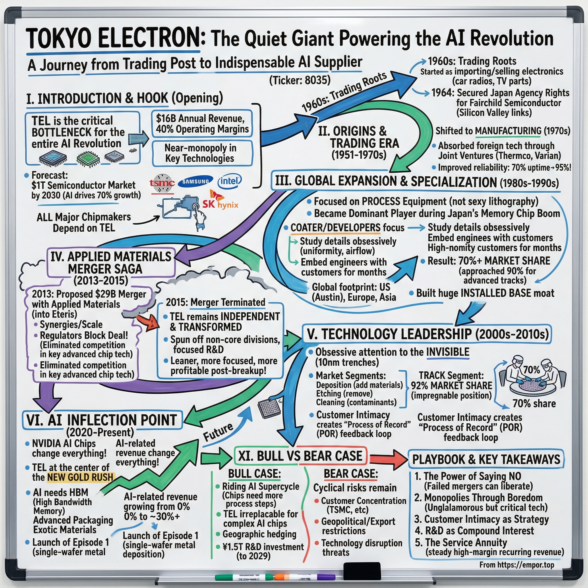
Tokyo Electron: The Quiet Giant Powering the AI Revolution
I. Introduction & Opening Hook
Picture this: In a gleaming cleanroom in Taiwan, an engineer in a bunny suit carefully loads a silicon wafer into a machine the size of a small apartment. This machine—a Tokyo Electron coater/developer—will apply photoresist with nanometer precision, enabling the creation of chips that power everything from your iPhone to ChatGPT's servers. There's a 92% chance this critical step uses TEL equipment. No other company comes close.
How did a Japanese trading company that started selling radios and car parts in the 1960s become the world's most dominant player in semiconductor equipment, with near-monopolistic positions in technologies that didn't exist when it was founded?
The answer reveals one of the most underappreciated stories in technology—a company that generates $16 billion in annual revenue, commands 40% operating margins, and stands as the critical bottleneck for the entire AI revolution, yet remains virtually unknown outside semiconductor circles.
Tokyo Electron Limited, trading as 8035.T on the Tokyo Stock Exchange, was incorporated in 1963 (though its predecessor dates to 1951). Today, as semiconductor giants race to build AI chips that require ever-more-complex manufacturing processes, TEL finds itself in an extraordinary position. The company forecasts the global semiconductor market will surpass $1 trillion by 2030, with AI-related semiconductors driving 70% of that growth. Every major chipmaker—TSMC, Samsung, Intel, SK Hynix—depends on TEL's equipment to manufacture their most advanced products.
This is the story of how a company built monopolies by being boring, survived a merger that would have destroyed its culture, and positioned itself as the indispensable supplier to the AI age. It's a masterclass in focus, patience, and the compound power of technical excellence—the kind of story that would make Warren Buffett smile and venture capitalists scratch their heads.
II. Origins & The Trading Company Era (1951-1970s)
The streets of Tokyo in 1963 buzzed with construction cranes and the hum of economic optimism. Japan was hosting the Olympics the following year, bullet trains were about to debut, and the country was transforming from post-war recovery into technological ambition. In a modest office building, two men were about to create something that would outlast all of it.
Tokyo Electron's founding wasn't born from a garage startup myth or a dropout's rebellion. It emerged from something distinctly Japanese: the calculated vision of Tokyo Broadcasting System (TBS) and Tokio Marine & Fire Insurance Company, who saw opportunity in importing and distributing foreign technology to feed Japan's industrial hunger. The company initially focused on importing and selling electronic components—everything from car radios to television parts.
But the real story begins with a fateful meeting in 1964. TEL's founders secured the Japan agency rights for Fairchild Semiconductor's products—the same Fairchild that spawned Intel, AMD, and the entire Silicon Valley ecosystem. While their American counterparts were inventing the future, TEL was learning how to sell it, service it, and eventually, how to build the machines that would make it.
Japan's post-war industrial policy created the perfect incubator. The government's technology importation strategy meant foreign companies needed local partners. TEL became the bridge—not just distributing products but absorbing knowledge, studying manufacturing processes, and building relationships with engineers who would later become customers.
By the early 1970s, a transformation was underway. TEL's leadership recognized that simply trading equipment would never build lasting value. They needed to manufacture. The company made its first major pivot, entering the semiconductor manufacturing equipment market with a focus on photolithography equipment. This wasn't random—they had watched their customers struggle with inconsistent equipment quality and realized the opportunity to do better.
The approach was quintessentially Japanese: license the technology, study it obsessively, improve it incrementally, and build trust through reliability. TEL formed joint ventures with American companies like Thermco Systems and Varian Associates, absorbing their technology while contributing Japanese manufacturing discipline. One early customer recalled: "The American equipment worked 70% of the time. The TEL-modified versions worked 95% of the time. In semiconductor manufacturing, that difference is everything."
By the late 1970s, TEL had built its first wholly-owned manufacturing facility in Yamanashi Prefecture. The company that started as a trading house was becoming a technology company, setting the stage for a transformation that would reshape the global semiconductor industry.
III. The Global Expansion & Specialization Era (1980s-1990s)
The year 1986 marked a turning point. The New York Times profiled Tokyo Electron as "a maker of semiconductor manufacturing equipment"—no longer just a distributor, but a manufacturer commanding respect from Silicon Valley to Seoul. The transformation was complete, but the real growth was just beginning.
Japan's semiconductor industry was on fire. Companies like NEC, Toshiba, and Hitachi were challenging American dominance in memory chips, and they needed equipment—lots of it. TEL found itself in the perfect position: a Japanese company with deep American technology connections, trusted by both sides of the Pacific.
The numbers told the story. By 1990, TEL was competing head-to-head with Dai Nippon Screen and Silicon Valley Group as the largest producer of semiconductor equipment globally. But while competitors fought across multiple fronts, TEL made a strategic decision that would define its future: focus on process equipment, not lithography.
"Everyone wanted to build lithography systems—that was the sexy technology," recalled a former TEL executive. "But we looked at the market and saw something different. For every lithography step, you need multiple process steps—coating, developing, etching, deposition. The market was bigger, stickier, and less crowded."
This focus paid off spectacularly in one product category: coater/developers. These machines apply and develop photoresist, the light-sensitive material that enables pattern transfer in chip manufacturing. It's not glamorous—think of it as the preparation and developing steps in photography—but it's absolutely critical. Every single chip needs it, and if it's done wrong, millions of dollars in wafers become expensive coasters.
TEL's engineers obsessed over details others ignored. They studied how photoresist flowed at different temperatures, how humidity affected adhesion, how to achieve perfect uniformity across 300mm wafers. They embedded engineers at customer sites, sometimes for months, studying problems and iterating solutions. When a major memory manufacturer struggled with yield issues, TEL engineers literally lived in the fab for three months until they solved it.
The 1990s brought geographic expansion. TEL established operations in the United States, opening a major facility in Austin, Texas—not coincidentally located near major customers like AMD and Motorola. European operations followed, with facilities in Ireland and Germany. But expansion wasn't just about sales offices; TEL built local service and applications centers, recognizing that semiconductor equipment isn't just sold—it's continuously optimized.
In Asia, TEL's timing was perfect. As Taiwan's TSMC and UMC emerged as foundry giants, and South Korea's Samsung and SK Hynix dominated memory, TEL was there from the beginning. The company didn't just sell equipment; it became a technology partner, co-developing processes that would become industry standards.
The results spoke volumes. By the late 1990s, TEL's coater/developer market share exceeded 70%. In certain segments, like tracks for advanced lithography, it approached 90%. Competitors found themselves in an impossible position: TEL's installed base was so large, and its process knowledge so deep, that customers wouldn't risk switching.
IV. The Applied Materials Merger Saga: Almost Creating a Monster (2013-2015)
September 24, 2013. In simultaneous press conferences in Tokyo and Santa Clara, two CEOs made an announcement that sent shockwaves through the semiconductor industry. Tokyo Electron and Applied Materials—the two largest semiconductor equipment companies—would merge into a new entity called Eteris. The $29 billion deal would create a behemoth controlling 25% of the global market.
The logic seemed irrefutable. Applied Materials CEO Gary Dickerson and TEL CEO Tetsuro Higashi painted a picture of synergies and scale. The combined company would have $3.5 billion in annual R&D spending, presence in every major process step, and the leverage to accelerate innovation. For Applied, it offered a tax-efficient structure (technically a merger of equals with headquarters in the Netherlands). For TEL, it promised access to Applied's strength in deposition and etch.
"We're creating the Bell Labs of semiconductor equipment," Dickerson proclaimed. The companies identified $500 million in annual cost synergies, with virtually no product overlap. Customers would benefit from integrated solutions. Shareholders would benefit from pricing power. Everyone wins.
Except regulators saw something different.
Behind closed doors at the Department of Justice, antitrust lawyers were building a different narrative. Their analysis revealed that in several critical technologies—particularly equipment for making advanced logic chips—Applied and TEL were the only two companies with the capability to compete at the leading edge. The merger wouldn't just reduce competition; it would eliminate it.
The companies tried everything. They offered to divest certain product lines. They proposed behavioral remedies. They flew executives to Washington repeatedly. But by April 2015, after 18 months of negotiations, the message from DOJ was clear: no remedy would be sufficient.
Acting Assistant Attorney General Renata B. Hesse didn't mince words: "The proposed merger would have combined the two largest competitors with the necessary know-how, resources and ability to develop and supply high-volume non-lithography semiconductor manufacturing equipment."
On April 27, 2015, the merger was officially terminated. Wall Street was disappointed. Some TEL employees were devastated—they had spent two years planning for integration. But something unexpected happened in the aftermath.
Forced to remain independent, TEL underwent a transformation that might never have occurred otherwise. During merger negotiations, the company had spun off its trading house and solar cell divisions to focus on semiconductor equipment. Post-breakup, this focus intensified. Management, freed from integration planning, doubled down on R&D. The company restructured operations, streamlined decision-making, and accelerated product development.
The numbers tell the story. In 2013, TEL's operating margin was 12%. By 2018, it exceeded 25%. Revenue grew from $5 billion to over $10 billion. The company that emerged from the failed merger was leaner, more focused, and more profitable than either company had been before.
"The failed merger was the best thing that never happened to us," reflected a senior TEL executive years later. "It forced us to confront our weaknesses, focus on our strengths, and prove we could win on our own. Applied is a great company, but we would have lost our soul in that merger."
V. Technology Leadership & Product Evolution (2000s-2010s)
Inside TEL's Miyagi Technology Center, a team of engineers huddles around a computer screen displaying microscopic images that look like alien landscapes. They're examining the sidewall of an etched trench just 10 nanometers wide—smaller than most viruses. The angle is off by 0.5 degrees. In the world of semiconductor manufacturing, that's the difference between a functioning chip and expensive scrap.
This obsessive attention to the invisible has driven TEL's product evolution for two decades. The company operates primarily in three segments: deposition (adding materials), etching (removing materials), and cleaning (removing contaminants). But it's in the Track segment—coater/developers and their associated processes—where TEL has built an almost impregnable position.
The dominance didn't happen overnight. It was built through thousands of incremental innovations, each solving problems customers didn't even know they had yet. When the industry moved from 200mm to 300mm wafers, TEL didn't just scale up its equipment—it reimagined the entire process flow. When extreme ultraviolet (EUV) lithography finally became viable, TEL had already spent a decade preparing coater/developers specifically optimized for EUV's unique requirements.
The numbers are staggering: 92% market share in coater/developers, 70% in wafer probers, dominant positions in single-wafer deposition. How does a company achieve such dominance in a high-tech industry? The answer lies in something the semiconductor industry calls "Process of Record" (POR).
Once a chipmaker qualifies a piece of equipment for a specific process, changing it risks months of requalification and potentially billions in lost revenue if yields drop. TEL understood this dynamic better than anyone. They didn't just sell equipment; they embedded themselves in their customers' process development. When Intel was developing its 14nm process, TEL engineers were there from day one. When TSMC pushed to 7nm, TEL's applications team had already run thousands of test wafers.
This customer intimacy created a powerful feedback loop. Each new process node generated learning that improved the next generation of equipment. TEL's R&D spending—consistently above 8% of sales—wasn't just about inventing new technologies; it was about solving specific customer problems before they became critical.
Consider the CLEAN TRACK™ LITHIUS Pro™ Z, launched in the early 2010s. To outsiders, it's just another coater/developer. To process engineers, it represented dozens of innovations: advanced temperature control that reduced defects by 30%, new nozzle designs that cut chemical consumption by 20%, throughput improvements that processed an extra 20 wafers per hour. Each improvement sounds minor. Together, they meant the difference between profitable and unprofitable chip production.
The company's approach to innovation was distinctly Japanese yet globally minded. While Silicon Valley equipment makers often pursued radical innovations, TEL focused on kaizen—continuous improvement. They would spend years perfecting the laminar flow in a cleaning chamber or optimizing the uniformity of film deposition. Boring? Perhaps. Profitable? Absolutely.
By 2015, TEL's installed base exceeded 70,000 units globally. Each machine generated not just equipment revenue but a stream of service, upgrades, and spare parts revenue that could last 20 years. This installed base became a moat—customers couldn't switch without replacing entire process flows, and TEL's deep process knowledge made switching even riskier.
VI. The AI Inflection Point (2020-Present)
The Nvidia GTC conference in March 2024 felt different. Jensen Huang, leather jacket gleaming under stage lights, unveiled the Blackwell GPU—a chip containing 208 billion transistors, manufactured using TSMC's most advanced process, consuming 1,200 watts of power. In the audience, TEL executives weren't watching the chip; they were calculating the equipment orders that would follow.
The AI revolution isn't just changing software—it's fundamentally transforming semiconductor manufacturing. AI chips require different architectures, different materials, and most importantly for TEL, different manufacturing processes. The company that spent decades perfecting equipment for logic and memory chips suddenly found itself at the center of a new gold rush.
The transformation began subtly in 2020-2021, when the industry experienced 26% annual growth. But by 2023, the impact was unmistakable. ChatGPT's launch didn't just change how we think about AI—it changed how chipmakers think about capacity. Every hyperscaler—Amazon, Google, Microsoft, Meta—began ordering AI accelerators by the hundreds of thousands.
These aren't your standard chips. AI processors require High Bandwidth Memory (HBM), advanced packaging, and exotic materials. Each requirement plays to TEL's strengths. HBM manufacturing needs precisely controlled deposition and etching processes—TEL equipment. Advanced packaging requires ultra-clean wafer preparation—TEL's specialty. The new materials need novel deposition techniques—exactly what TEL's been developing.
"The trend of generative AI like ChatGPT has already driven the demand for semiconductor equipment," TEL President Toshiki Kawai noted in a recent earnings call. But this understates the transformation. TEL's revenue from AI-related semiconductor equipment has grown from virtually nothing to 30% of total sales, heading toward 40% by March 2026.
The company's July 2024 launch of Episode™ 1 exemplifies this AI-driven innovation. This single-wafer metal deposition platform can integrate up to 8 process modules—double its predecessor's capacity. Why does this matter? AI chips require complex metal interconnects to move data between billions of transistors. Episode™ 1 can deposit different metals in sequence without breaking vacuum, reducing defects and increasing yield—critical for chips that can cost $30,000 each.
The numbers are extraordinary. TEL's net sales rose 32.8% year-on-year to ¥2.43 trillion ($15.7 billion) in fiscal 2024, with operating profit hitting ¥697.3 billion ($4.5 billion). The operating margin of 28.7% would make software companies jealous. But what's driving this isn't just volume—it's value. AI chips are larger, more complex, and require more process steps. Each chip might need 3,000 individual process steps, compared to 1,500 for a standard processor. More steps mean more equipment, more service, more revenue for TEL.
The geographic distribution tells another story. While China restrictions have grabbed headlines, TEL's exposure has actually decreased as Taiwan, South Korea, and Japan have ramped up AI chip production. TSMC alone accounts for over 90% of AI chip manufacturing, and they're TEL's largest customer. Samsung's aggressive HBM expansion, Intel's foundry ambitions, and Japan's Rapidus project all rely heavily on TEL equipment.
Looking ahead, TEL management sees AI driving a fundamentally different semiconductor cycle. Traditional boom-bust patterns driven by consumer electronics are being replaced by steady, structural growth in datacenter investment. As Kawai stated, "Advanced logic ICs for data centers, as well as memory chips for AI smartphones and AI PCs, are expected to drive double-digit growth in the semiconductor equipment market by 2026."
VII. Financial Performance & Market Position
The numbers coming out of TEL's Akasaka headquarters in fiscal 2024 would make any CFO envious: ¥2.43 trillion in revenue, ¥697.3 billion in operating profit, and perhaps most remarkably, a return on equity exceeding 30%. For a capital-intensive manufacturing company, these aren't just good numbers—they're exceptional.
But the real story isn't in the headlines; it's in the composition. TEL's revenue breaks down across multiple segments, each with different dynamics. The SPE (Semiconductor Production Equipment) segment generates roughly 95% of revenue, with Field Solutions (service and modifications) contributing the remainder. Within SPE, the mix tells the story of technological evolution: deposition equipment (32%), etch systems (28%), track equipment (25%), and cleaning systems (15%).
What makes TEL's financial model particularly powerful is the recurring nature of much of its revenue. While new equipment sales grab attention, the installed base of over 70,000 units generates a steady stream of service revenue, spare parts, and upgrades. This service revenue—typically 25-30% of total sales—carries higher margins and provides stability during industry downturns.
The company's stated ambition is breathtaking: invest ¥1.5 trillion ($9.5 billion) in R&D by March 2029. That's not a typo—it represents nearly 10% of sales annually, a level that would concern most investors. But TEL's track record suggests this isn't speculation; it's calculated investment in maintaining technological moats.
Capital allocation has been equally disciplined. The company maintains a fortress balance sheet with net cash typically exceeding ¥500 billion, providing flexibility for both organic investment and opportunistic M&A. Shareholder returns have been generous but measured—dividend payout ratios around 50%, supplemented by strategic buybacks when valuations compress.
The geographic revenue split reveals both opportunity and risk. Taiwan represents roughly 30% of sales (primarily TSMC), China 25%, South Korea 20%, with Japan, North America, and Europe comprising the balance. The China exposure has actually decreased from over 30% three years ago, as the company navigated export restrictions while maintaining critical customer relationships.
Market share data across segments shows the fruits of decades of focus. In coater/developers: 92%. In wafer probers: 70%. In single-wafer deposition: 45%. In batch processing: 40%. These aren't volatile positions—some have been stable for over a decade, protected by switching costs, process integration, and continuous innovation.
What's perhaps most impressive is margin progression. Operating margins have expanded from 12% a decade ago to nearly 30% today. This isn't financial engineering—it's operational excellence. Higher-value products, better capacity utilization, and service revenue growth have all contributed. The AI boom has accelerated this trend, as cutting-edge equipment commands premium pricing.
The forward outlook suggests this is just the beginning. TEL forecasts reaching ¥3 trillion in revenue by 2027, implying continued 10%+ annual growth. With the semiconductor equipment market expected to reach $150 billion by 2030, and TEL targeting increased share in high-growth segments like advanced packaging and EUV-related processes, the growth runway appears substantial.
VIII. Competitive Dynamics & Strategic Positioning
In the semiconductor equipment industry, the battle lines are clearly drawn. Applied Materials, the American giant, commands the broadest portfolio. Lam Research dominates etch. ASML owns lithography with its EUV monopoly. And TEL? TEL chose to win through depth, not breadth.
The competitive dynamics reveal a fascinating strategic puzzle. Applied Materials, with $27 billion in revenue, is nearly twice TEL's size. Yet in head-to-head competition in specific technologies, TEL often wins. The reason lies in focus. While Applied spans virtually every process technology, TEL concentrated its resources on select areas where it could achieve dominance.
This shows clearly in customer decisions. When TSMC was selecting equipment for its 3nm process, they could have standardized on Applied Materials for simplicity. Instead, they chose best-in-class for each process step: ASML for lithography, TEL for tracks, Lam for certain etch processes, Applied for specific deposition tools. TEL's specialization strategy paid off—they won not by being everything to everyone, but by being irreplaceable where they competed.
The innovation race intensifies with each node shrink. As Kawai noted, "Advanced logic ICs for data centers, as well as memory chips for AI smartphones and AI PCs, are expected to drive double-digit growth in the semiconductor equipment market by 2026." This growth isn't just about capacity—it's about capability. Each new process node requires equipment that didn't exist two years prior.
Geopolitical tensions add another layer of complexity. Export restrictions on China have reshaped the competitive landscape. While Applied and Lam saw significant revenue impacts, TEL's exposure, though substantial, proved manageable. The company's "China Plus One" strategy—maintaining presence while diversifying growth—has proven prescient.
But the real competitive moat isn't technology or geography—it's customer intimacy. TEL embeds engineers at customer sites for years, learning not just what customers need today, but what they'll need in five years. When Samsung was developing its gate-all-around transistor technology, TEL engineers were there from concept to production, co-developing processes that became integral to the technology's success.
The emergence of Chinese equipment makers like NAURA and AMEC adds a new dimension. These companies, backed by government support and serving a protected domestic market, are moving up the technology curve. Yet TEL's position seems secure. The switching costs aren't just financial—they're existential. A yield drop of even 1% on leading-edge production could cost hundreds of millions in lost revenue.
Looking forward, the competitive dynamics appear to be shifting from market share battles to technology races. The industry predicts the semiconductor market will reach $5 trillion by 2050—ten times today's size. In this world, there's room for multiple winners, but only if they can keep pace with exponentially increasing complexity.
IX. The Future: Scaling for the AI Semiconductor Era
Standing in TSMC's Fab 18 in Taiwan—the world's most advanced semiconductor facility—you're witnessing the future being built one atomic layer at a time. The chips produced here will power AI systems we can barely imagine. And TEL's equipment enables nearly every critical process step.
The numbers are staggering. SEMI predicts the semiconductor market will reach $5 trillion by 2050—ten times today's size. TEL's CEO Toshiki Kawai is even more specific: AI will dominate 70% of the semiconductor market by 2030. This isn't incremental growth; it's a fundamental reshaping of the industry.
The technology roadmap beyond 2nm presents challenges that would have seemed impossible a decade ago. Transistors are approaching atomic scales where quantum effects dominate. Traditional scaling is ending, replaced by new architectures: gate-all-around transistors, backside power delivery, 3D integration. Each innovation requires new manufacturing processes, and TEL is developing equipment for all of them.
Advanced packaging represents a particularly compelling opportunity. As chips reach the limits of monolithic scaling, the industry is turning to heterogeneous integration—combining multiple chips in sophisticated packages. This requires equipment that can handle wafer-level packaging, chip-to-wafer bonding, and through-silicon vias. TEL's acquisition of packaging-related technologies and its development of hybrid bonding equipment position it well for this transition.
Energy efficiency has become existential. Data centers already consume 2% of global electricity, and AI is accelerating this trend. TEL has committed to achieving net-zero emissions for scopes 1, 2, and 3 by 2040—ambitious for a manufacturing company. But it's also developing equipment that reduces power consumption in chip manufacturing by 30% and enables chips that are inherently more energy-efficient.
The sustainability challenge extends beyond energy. Semiconductor manufacturing consumes vast quantities of water and chemicals. TEL's newest cleaning systems reduce water usage by 40% while improving particle removal. Their closed-loop chemical recycling systems can recover and reuse 90% of certain process chemicals. These aren't just environmental nice-to-haves—they're becoming requirements as fabs face resource constraints.
The talent war represents another critical challenge. As semiconductor manufacturing becomes more complex, the industry needs engineers who understand quantum mechanics, materials science, and AI—often all three. TEL is investing heavily in university partnerships, establishing research centers near technical universities, and creating training programs that can take years to complete.
Geopolitical realignment continues reshaping the industry. The U.S. CHIPS Act, Europe's semiconductor initiative, and Japan's Rapidus project all aim to rebuild domestic semiconductor capabilities. TEL, with its global footprint and local presence, is well-positioned to support these initiatives while maintaining its critical relationships in Asia.
X. Playbook: Business & Investment Lessons
The TEL story offers a masterclass in building enduring technology companies, with lessons that extend far beyond semiconductors.
The Power of Saying No: The failed Applied Materials merger could have been devastating. Instead, it became liberation. By being forced to remain independent, TEL discovered strengths it might never have developed. The lesson: sometimes the best deals are the ones you don't make. The company that emerged from the failed merger was leaner, more focused, and ultimately more valuable than the combined entity would have been.
Monopolies Through Boredom: TEL built dominant positions not in sexy technologies but in processes everyone needs but nobody talks about. Coater/developers aren't revolutionary—they're essential. By focusing on technologies that are critical but unglamorous, TEL faced less competition and built deeper moats. The highest returns often come from the most boring businesses.
Customer Intimacy as Strategy: TEL doesn't just sell equipment; it embeds itself in customers' process development. Engineers spend months at customer sites, learning problems before they become critical. This isn't customer service—it's strategic intelligence. The deepest moats are built on relationships, not just technology.
R&D as Compound Interest: Spending 8-10% of revenue on R&D seems excessive until you realize it's the source of TEL's pricing power. Each generation of equipment builds on decades of accumulated knowledge. Like compound interest, the returns accelerate over time. Patient capital deployed consistently beats moonshot bets.
Geographic Hedging: While competitors concentrated risk, TEL distributed it. No single geography represents more than 30% of revenue. When China restrictions hit, other markets compensated. In a globalized but fracturing world, geographic diversity isn't just risk management—it's option value.
The Service Annuity: New equipment sales get headlines, but service revenue pays bills. TEL's installed base generates predictable, high-margin revenue for decades. The lesson: in capital equipment, the sale is just the beginning of the customer relationship, not the end.
Capital Cycle Mastery: Semiconductor equipment is notoriously cyclical, but TEL has dampened volatility through mix management. When logic slows, memory often accelerates. When both slow, service revenue provides cushion. Understanding and preparing for cycles beats trying to predict them.
Technical Moats in Physical Products: In an era obsessed with software moats, TEL proves physical products can have equally powerful barriers. The combination of switching costs, process integration, and accumulated knowledge creates barriers that are nearly impossible to overcome.
XI. Bear vs. Bull Case Analysis
The Bull Case: Riding the AI Supercycle
The optimistic view starts with structural change. We're not in a typical semiconductor cycle—we're at the beginning of a transformation as significant as the internet revolution. AI isn't just another application; it's a general-purpose technology that will reshape every industry. McKinsey predicts AI could add $13 trillion to global GDP by 2030. Every dollar of that value requires semiconductors, and every semiconductor requires TEL equipment.
The numbers support this narrative. AI semiconductors are growing at 30% annually, far outpacing traditional semiconductors' 7% growth. These aren't just more chips—they're more complex chips requiring more process steps, more equipment, and more service. A traditional smartphone processor might require 1,500 process steps; an AI training chip requires 3,000. More steps equal more TEL revenue.
Market position provides another pillar of the bull case. With 92% share in coater/developers and dominant positions across multiple technologies, TEL has pricing power that's only increasing. As processes become more complex, switching costs rise exponentially. A customer might pay 10% more for TEL equipment to avoid the risk of yield loss from switching.
Geographic diversification is finally paying dividends. While China represented over 30% of revenue three years ago, it's now 25% and declining as other markets grow faster. Japan's Rapidus, U.S. reshoring, and European fab projects all represent incremental demand that didn't exist before.
The financial trajectory seems sustainable. Operating margins have expanded from 12% to nearly 30% over a decade, and management sees room for further improvement. With ¥1.5 trillion in planned R&D investment, TEL is betting on technology leadership extending its moats. The balance sheet, with over ¥500 billion in net cash, provides flexibility for both organic growth and strategic acquisitions.
The Bear Case: Cyclical Risks and Structural Threats
The pessimistic view starts with history. Semiconductor equipment has always been cyclical, and this time might not be different. The industry saw similar optimism during the internet boom, the mobile revolution, and the cloud buildout. Each ended with overcapacity and brutal downturns. AI could follow the same pattern.
Customer concentration presents real risks. TSMC alone represents roughly 20% of revenue. Samsung, Intel, and SK Hynix combined add another 30%. If any major customer cuts spending—due to overcapacity, technology transitions, or financial constraints—TEL's revenue could drop significantly. The company's operating leverage works both ways.
Geopolitical risks are escalating, not diminishing. Export restrictions could expand beyond current limitations. China is aggressively developing domestic equipment capabilities with unlimited government support. While Chinese equipment currently lags by several generations, the gap is closing. In commodity segments, Chinese competitors are already winning on price.
Technology disruption remains a constant threat. What if a breakthrough in quantum computing or optical computing obsoletes traditional semiconductors? What if new manufacturing techniques—molecular assembly, biological computing—bypass traditional equipment entirely? TEL's enormous installed base could become a liability rather than an asset.
Valuation poses another concern. At current multiples, the market is pricing in perfect execution for years. Any disappointment—a delayed product, a lost customer, a yield issue—could trigger significant multiple compression. The stock's volatility during previous downturns shows how quickly sentiment can shift.
The ESG challenge is real and growing. Semiconductor manufacturing is incredibly resource-intensive, consuming vast amounts of energy, water, and chemicals. While TEL has committed to net-zero by 2040, the path is unclear and likely expensive. Environmental regulations could significantly impact profitability.
XII. Final Reflections & Key Takeaways
Tokyo Electron is the company that nobody talks about but everybody depends on. Your smartphone, laptop, car, and soon your AI assistant all depend on chips made with TEL equipment. Yet outside semiconductor circles, the company remains virtually unknown. This anonymity might be its greatest strength.
The failed Applied Materials merger emerges as the defining moment in TEL's modern history. What seemed like catastrophe became catalyst. Forced to remain independent, TEL discovered reserves of innovation and efficiency it might never have tapped. The company that emerged wasn't just surviving—it was thriving with margins and growth that exceeded what the merged entity projected.
For founders and executives, TEL offers a different model of success. While Silicon Valley celebrates disruption and revolution, TEL built its empire through evolution and execution. They didn't invent the semiconductor; they perfected the tools to make them. They didn't create new markets; they dominated existing ones through patient excellence.
The investment lessons are equally compelling. In a world obsessed with software multiples and asset-light models, TEL proves that physical products can generate software-like returns. The combination of high market share, switching costs, and continuous innovation creates compounding advantages that accelerate over time.
Looking ahead, the question isn't whether TEL will grow, but how fast. Management's target of ¥3 trillion in revenue by 2027 implies continued double-digit growth. With AI driving semiconductor demand and new technologies requiring ever-more-complex manufacturing, the runway appears long.
Will TEL hit $50 billion in revenue by 2030? The math suggests it's possible. If semiconductors reach $1 trillion by 2030 as predicted, and equipment maintains its historical 15% share, that's a $150 billion market. TEL would need just 33% market share—not much above its current position—to reach that milestone.
But perhaps the most important lesson from TEL is about time horizons. The company spent decades building dominant positions in boring technologies. They invested through downturns, maintained R&D spending when competitors cut, and prioritized customer relationships over quarterly earnings. In an era of instant gratification, TEL proves that the biggest returns still come from patient capital deployed consistently over time.
The quiet giant from Tokyo has positioned itself at the center of the AI revolution not through luck or timing, but through decades of deliberate choices. Every chip powering our AI future will likely pass through TEL equipment. That's not just a business moat—it's a civilization-critical position.
As semiconductor manufacturing becomes more complex, more critical, and more valuable, the companies that enable it become increasingly important. TEL isn't just riding the AI wave; it's providing the surfboards. And in a world where every company is becoming a technology company, and every technology requires semiconductors, that might be the best position of all.
 RSS Feed
 Spotify
 Apple Podcasts
 Amazon Music
 Audible
 YouTube