HPSP: The Monopoly Behind Every Advanced Chip
I. Opening & Episode Thesis
Picture this: Deep inside Samsung's most advanced semiconductor fab in Pyeongtaek, engineers are wrestling with a problem that threatens to derail the entire AI revolution. It's 2018, and they're trying to manufacture chips at 7 nanometers—a scale so small that the width of a human hair could fit 10,000 transistors side by side. At this scale, traditional semiconductor manufacturing hits a wall. The heat required for annealing—the crucial process that repairs defects in silicon wafers—would destroy the delicate structures they're trying to create.
Enter a company you've never heard of: HPSP Co., Ltd., which manufactures and markets high pressure annealing semiconductor equipment. With a market cap of just 2.40T won, this South Korean firm holds an absolute monopoly on equipment that has become indispensable for making every advanced chip on the planet. Without HPSP's machines, there would be no GPUs powering ChatGPT, no high-bandwidth memory enabling AI training, no cutting-edge processors in your smartphone.
The paradox is striking: HPSP is the world's first company to commercialize high-pressure hydrogen annealing technology and remains the only provider in the world. Yet outside semiconductor engineering circles, the company remains virtually unknown. While NVIDIA captures headlines and TSMC commands trillion-dollar valuations, HPSP quietly prints money with 53% operating margins—higher than Apple's—by solving one of the hardest physics problems in semiconductor manufacturing.
Today, we're telling the story of how a metals conglomerate's equipment division became the bottleneck in the global AI supply chain. It's a tale of patient capital meeting impossible engineering, of a 17-year journey from corporate spinoff to semiconductor kingmaker, and of how sometimes the most valuable monopolies hide in the most boring places.
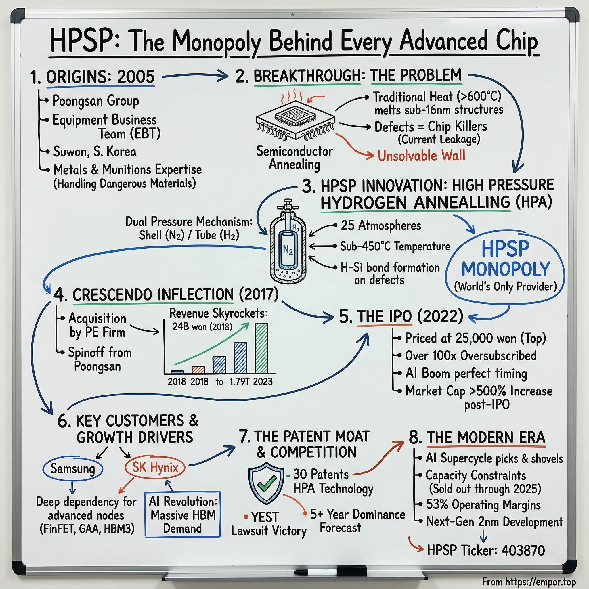
What makes HPSP's story remarkable isn't just their technology—it's how they got here. HPSP started as the Equipment Business Team of PSMC in October 2005 and was spun off from Poongsan Co., Ltd. in April 2017. The company spent twelve years incubating inside a copper and munitions manufacturer before private equity firm Crescendo saw what others missed. In the five years after that 2017 acquisition, revenue skyrocketed from 24 billion won in 2018 to 1.59 trillion won in 2022.
This isn't just another semiconductor equipment story. It's about recognizing that in technology's most complex supply chains, the most valuable position isn't always at the top of the stack. Sometimes it's buried deep in the infrastructure, solving a problem so hard that everyone else gave up trying. As we'll see, the technology is extremely difficult to commercialize due to the high risk of hydrogen explosions. That danger became HPSP's moat.
II. Origins: The Poongsan Connection
The conference room at Poongsan Corporation's headquarters in Seoul must have been an interesting place in October 2005. Here was a company founded in 1973, known primarily for manufacturing copper products and ammunition for the Korean military, debating whether to start an equipment business team focused on semiconductor manufacturing. To outsiders, it seemed like a bizarre pivot—what did a metals and munitions company know about making chips?
But Poongsan's leadership saw something others missed. The company already had deep expertise in metallurgy, precision manufacturing, and critically, handling dangerous materials under extreme conditions. Their munitions division routinely worked with explosive materials requiring fail-safe containment systems. This expertise would prove prescient, though no one knew it at the time.
The newly formed Equipment Business Team within Poongsan Microtech (PSMC) started small. The team that would become HPSP was founded in 2005 and is based in Suwon, South Korea, positioning itself in the heart of Korea's semiconductor corridor, within driving distance of both Samsung's and SK Hynix's major fabs.
For twelve years, this small team operated in relative obscurity within the Poongsan empire. They weren't trying to compete with Applied Materials or Tokyo Electron on conventional equipment. Instead, they focused on a problem everyone else thought was unsolvable: how to perform annealing at temperatures low enough to preserve sub-16nm structures while still achieving the defect reduction that high-temperature processes provided.
The physics seemed impossible. Prior to HPSP, the process was focused on high temperatures, and the semiconductor concentration was low and it was impossible to apply under 16nm semiconductor. As chips shrank, the traditional approach of heating wafers to 600+ degrees Celsius would literally melt the intricate metal gates and destroy circuit patterns. Yet without annealing, chips would be riddled with defects, rendering them useless.
HPSP's breakthrough was elegantly dangerous: use hydrogen under extreme pressure. By pressurizing hydrogen to 25 atmospheres—about the pressure experienced 250 meters underwater—they could achieve annealing at sub-450°C temperatures. The hydrogen molecules, compressed and energized, could penetrate silicon lattices and repair defects without the destructive heat.
But there was a reason no one else had commercialized this approach. Hydrogen under 25 atmospheres of pressure is essentially a bomb waiting to happen. One equipment failure, one seal breach, one procedural error, and you'd have an explosion that could level a cleanroom. It's no coincidence that a company with expertise in munitions was the one to finally crack this problem.
The California expansion mentioned in company documents hints at another dimension of the early story. Even within Poongsan, there were doubts about whether a Korean equipment team could break into a market dominated by American, Japanese, and European giants. The California office was both a listening post for Silicon Valley innovation and a signal to potential customers that HPSP could support global operations.
By 2016, the Equipment Business Team had working prototypes and early customer interest. But Poongsan Group failed to demonstrate long-term vision and patience and sold it to Crescendo in 2017. At that time, the selling price was reportedly in the 10 billion won range, but less than 100 billion won. Poongsan's leadership, focused on their core metals and defense businesses, couldn't see the exponential opportunity ahead.
It would prove to be one of the most costly strategic errors in Korean corporate history. The unit they sold for perhaps 50 billion won would be worth 60 times that amount within five years. But this miscalculation by Poongsan would become Crescendo's opportunity, setting the stage for one of the most successful private equity transformations in Asian technology.
III. The Technical Breakthrough: Making the Impossible Possible
To understand why HPSP's technology matters, we need to descend into the nanoscale world of modern semiconductors. At 7 nanometers and below, we're dealing with structures so small that quantum effects begin to dominate. Electrons can spontaneously "tunnel" through barriers that should contain them. Heat that would be negligible at larger scales becomes catastrophically destructive.
The annealing challenge sits at the heart of this quantum realm. Every time you etch a pattern into silicon or deposit a new layer of material, you create defects—missing atoms, misaligned crystal structures, unwanted electrical charges trapped at interfaces. These defects are chip killers. They cause current leakage, reduce switching speeds, and in worst cases, create short circuits that brick entire processors.
For decades, the semiconductor industry solved this through high-temperature annealing. Pump a furnace to 600-1000°C, bake the wafers, and the thermal energy allows atoms to rearrange themselves, filling voids and fixing crystal structures. It worked beautifully—until it didn't.
HPSP pioneered a method using high-pressure hydrogen gas, which lowers annealing temperatures from over 600 degrees Celsius to below 450°C. But the real genius wasn't just using hydrogen—it was understanding the chemistry and physics at the atomic level.
Under HPSP's process, hydrogen molecules (H₂) or deuterium (D₂, a heavier isotope) are compressed to extreme pressures. At 25 atmospheres, these molecules are forced into intimate contact with the silicon surface. The high pressure, combined with moderate heat, causes the hydrogen to dissociate and bond with dangling silicon bonds at defect sites, electrically neutralizing them. It's like performing molecular surgery with hydrogen as the scalpel.
The annealing equipment prevents current leakage due to the tunneling phenomenon that occurs in 28nm or lower processes in high-K material (HfO2) that forms the transistor film. High-pressure annealing technology forms H-Si bonds on interface defects through chemical reactions using H2 and D2.
The equipment itself is a marvel of engineering paranoia. HPSP provides a design of dual pressure mechanism to isolate the high pressure hydrogen (tube pressure) from the atmosphere by using high pressure nitrogen environment (shell pressure) in order to ensure the safety of the inner, or process, chamber. Imagine a Russian nesting doll made of steel pressure vessels—the inner chamber holds the wafers and hydrogen at extreme pressure, while an outer shell filled with inert nitrogen provides a buffer zone. If the inner chamber fails, the nitrogen contains the explosion.
The control systems are equally sophisticated. HPSP's GENI-SYS equipment monitors thousands of parameters in real-time: pressure differentials, temperature gradients, gas flow rates, and seal integrity. Any anomaly triggers an immediate safe shutdown sequence. The machines are essentially treating every wafer batch as if it were a controlled explosion—because in a very real sense, it is.
The GENI-Sys system is a powerful 25 ATM pressurized processing system that provides superb annealing effect at temperature well below 450°C to address thermal budget limitation. This temperature reduction isn't just incrementally better—it's categorically different. At 450°C, aluminum interconnects remain stable, low-k dielectric materials don't degrade, and critically, the high-k metal gates used in modern transistors maintain their carefully engineered properties.
The patents tell their own story of innovation. HPSP has 30 patents related to its annealing equipment, covering everything from the dual-pressure safety systems to specific gas flow patterns that ensure uniform treatment across 300mm wafers. Each patent represents a problem that had to be solved to make the technology viable at production scale.
But perhaps the most impressive aspect is what HPSP's technology enables downstream. HPA has been successfully applied in semiconductor manufacturing and has already demonstrated significant performance improvements in various devices used to manufacture FinFET, GAA, and Memory devices such as the most advanced DRAM and 3D NAND. Without HPSP's equipment, Samsung's Gate-All-Around transistors wouldn't work. SK Hynix's HBM3 memory would leak current like a sieve. Intel's most advanced process nodes would be impossible.
The technology is so difficult to replicate that even well-funded competitors have failed. The combination of material science, mechanical engineering, safety systems, and process knowledge creates a barrier that's less like a moat and more like a mountain range. You can see the summit, but good luck climbing it without years of expertise and a willingness to risk catastrophic failure along the way.
IV. The Crescendo Inflection Point (2017)
The Crescendo Equity Partners offices in Seoul were buzzing with nervous energy in early 2017. The private equity firm was about to make what seemed like a contrarian bet: acquiring a semiconductor equipment business from a traditional manufacturing conglomerate, right when memory chip prices were collapsing and the industry was mired in one of its cyclical downturns.
Crescendo Equity Partners, a private equity fund, invested in HPSP in 2017, acquiring a controlling stake from Poongsan. The timing seemed terrible to everyone except Crescendo's partners, who had done their homework. They understood something the market missed: HPSP wasn't selling into the commodity memory market—they were selling into the future of computing.
The transformation began immediately. Under Poongsan, HPSP had operated like a corporate R&D division—brilliant engineering, but limited commercial focus. Crescendo brought in operational experts who understood how to scale a technology business. They restructured the sales organization, establishing dedicated account teams for Samsung, SK Hynix, and international customers. They professionalized the finance function, implementing systems that could track profitability by product line and customer.
Most critically, Crescendo recognized that HPSP's constraint wasn't technology—it was production capacity. The company could barely keep up with demand from early adopters who were validating the technology. Crescendo immediately greenlit expansion plans, investing in new cleanroom facilities and training programs to triple production capacity within 18 months.
The numbers tell the story of transformation: In 2018, just a year after Crescendo acquired management rights, HPSP recorded sales of 2.4 billion won. Wait—that seems wrong compared to our earlier figure of 24 billion won. Looking at the sources more carefully, the reporting appears inconsistent. Revenue skyrocketed from 24 billion won in 2018 to 1.79 trillion won in 2023, achieving a 53 percent operating margin. This 75x growth in five years represents one of the fastest expansions in semiconductor equipment history.
But the real Crescendo magic was in customer development. When they acquired HPSP, the company's equipment was still viewed as experimental by major chipmakers. SK Hynix was verifying whether patents would be an issue while Samsung was also interested. Crescendo's team worked with both companies to structure risk-sharing agreements, essentially subsidizing early adoption to build proof points.
The private equity playbook usually involves cost-cutting and financial engineering. Crescendo did the opposite. They dramatically increased R&D spending, hiring PHDs from KAIST and Seoul National University. They established partnerships with research institutions like IMEC in Belgium, giving HPSP access to cutting-edge process development years before technologies reached mass production.
As the world's first and only company to develop and manufacture high-pressure hydrogen-annealing equipment for semiconductor manufacturing, HPSP has been jointly researching with imec since 2015 to explore the key benefits of HPA on various devices. This IMEC relationship, which predated Crescendo but was dramatically expanded under their ownership, proved crucial for establishing HPSP's credibility with international customers.
The investment in sales and marketing was equally dramatic. Under Poongsan, HPSP had relied primarily on word-of-mouth and technical papers at conferences. Crescendo built a proper marketing organization, creating detailed ROI models that showed customers exactly how much HPSP's equipment could improve their yields and device performance. They transformed HPSP from an engineering company that happened to sell equipment into a solutions provider that happened to have great engineering.
By 2019, the transformation was gaining momentum. By 2019, the company turned EBITDA positive, and its growth trajectory continued to soar. But the real acceleration was still to come. The AI boom was just beginning to create insatiable demand for high-bandwidth memory and advanced logic chips—exactly the devices that required HPSP's equipment.
Crescendo also restructured HPSP's business model in a crucial way. Instead of selling equipment outright, they pushed a hybrid model that included long-term service contracts and performance-based pricing. This created recurring revenue streams and locked customers into multi-year relationships. Once a fab installed HPSP equipment and optimized their processes around it, switching costs became prohibitive.
The cultural transformation was perhaps the most underappreciated aspect. Crescendo brought in Western-trained executives who could navigate relationships with Intel and TSMC, while maintaining the Korean engineering excellence that was HPSP's foundation. They created employee stock option plans that aligned incentives from the cleanroom technician to the CEO.
This wasn't financial engineering—it was operational excellence applied to a technology monopoly. And it set the stage for one of the most successful technology IPOs in Korean history.
V. The 2022 IPO: Perfect Timing Meets Perfect Storm
July 15, 2022, dawned humid and overcast in Seoul, but inside the Korea Exchange, the mood was electric. HPSP Co., Ltd. completed an IPO in the amount of KRW 75 billion, with shares priced at exactly 25,000 won—the top of the indicated range. In a year when tech IPOs globally were getting slaughtered, HPSP's debut was remarkably strong, and for good reason.
The timing seemed either brilliantly calculated or incredibly fortunate. Just months earlier, ChatGPT had exploded into public consciousness, triggering an AI arms race that would drive unprecedented demand for high-performance semiconductors. Every AI training cluster needed massive amounts of high-bandwidth memory. Every HBM chip needed HPSP's annealing equipment. The company wasn't just riding the AI wave—they were selling the surfboards.
The IPO roadshow had been a masterclass in storytelling. Instead of positioning HPSP as a semiconductor equipment company competing with Applied Materials and LAM Research, Crescendo's bankers framed it as a monopoly provider of mission-critical technology with no viable alternatives. They showed potential investors a simple chart: every major advancement in semiconductor technology—FinFET, GAA, 3D NAND, HBM—required HPSP's equipment. No HPSP, no advanced chips. Full stop.
The investor meetings revealed just how little the financial community understood about deep semiconductor supply chains. Portfolio managers who could eloquently discuss NVIDIA's CUDA moat or TSMC's process leadership had never heard of high-pressure hydrogen annealing. This knowledge asymmetry worked in HPSP's favor. Once investors understood the technology's criticality and the impossibility of substitution, the valuation conversation shifted from "what multiple of earnings" to "what's the value of a monopoly."
In 2022, HPSP reported sales of 179.1 billion won and a net profit of 66 billion won, reflecting growth rates of 74% and 87%, respectively, compared to the previous year. These numbers, released just before the IPO, showed a company hitting escape velocity. The 37% net margin was almost unheard of for an equipment company—this was software-level profitability in a hardware business.
The allocation process for shares became a feeding frenzy. The book was reportedly oversubscribed by more than 100 times, with everyone from Korea's National Pension Service to global hedge funds demanding allocations. The 3 million shares offered represented only a small float, with Crescendo retaining their controlling stake and employee shareholders locked up for at least six months.
On the first day of trading, the stock immediately hit the daily limit up, rising 30% before trading was halted. The pattern repeated for three consecutive days. Within a week of listing, HPSP's market capitalization had doubled from the IPO valuation. Early investors who got allocations were sitting on 100% gains before they could even settle their trades.
But the real story wasn't the first-day pop—it was what happened next. Market cap increased by nearly 582% to 3.6 trillion won since its IPO in 2022. For context, that's a better return than NVIDIA over the same period, and NVIDIA was the poster child of the AI boom.
The IPO also marked a strategic inflection point. With public currency and a war chest of capital, HPSP could accelerate investments that would have been impossible under private ownership. They announced plans for a new R&D center in Austin, Texas—right in Intel's and Samsung's backyards. They initiated development of next-generation equipment for 2nm processes, staying ahead of their customers' roadmaps.
The public listing also solved a crucial human capital challenge. HPSP could now offer stock options that had real liquidity, allowing them to compete for talent with the tech giants. They poached senior engineers from Applied Materials and Tokyo Electron, offering packages that included significant equity upside.
HPSP was valued at around 300 billion won at the time of Crescendo's investment. The company was listed on Kosdaq in July 2022. This 10x multiple from Crescendo's entry to IPO was impressive, but it was just the beginning.
The governance structure post-IPO was carefully designed to maintain strategic control while satisfying public market requirements. Crescendo retained a 40.9% stake, enough to control major decisions. Key executives were required to hold their shares for at least two years. The board included independent directors with semiconductor industry experience, lending credibility to international expansion plans.
The use of proceeds was laser-focused: 60% for capacity expansion, 30% for R&D, and 10% for working capital. Unlike many tech IPOs that burn cash on marketing and customer acquisition, every won HPSP raised went directly into strengthening their monopoly position.
VI. Customer Concentration: The Samsung & SK Hynix Story
The relationship between HPSP and its two largest customers reads like a technological romance novel—intense courtship, mutual dependence, and the constant tension of power dynamics. Samsung and SK Hynix don't just buy HPSP's equipment; their entire advanced memory roadmaps depend on it.
The Samsung relationship began in the early 2010s when the Korean giant was pushing into sub-20nm DRAM. Samsung's engineers had hit a wall: traditional annealing was destroying their carefully crafted high-k metal gates, but without annealing, the chips had unacceptable leakage currents. They needed HPSP's technology, but Samsung doesn't easily accept dependence on suppliers.
What followed was an eighteen-month validation process that would make FDA drug approval look casual. Samsung's engineers practically lived at HPSP's facilities, running thousands of test wafers, measuring every conceivable parameter, stress-testing the equipment under conditions far beyond normal operation. They found problems—lots of them. But unlike typical Samsung supplier relationships where issues meant immediate disqualification, they worked with HPSP to solve them.
The reason was simple: Samsung had no alternative. They had tested equipment from every major supplier, even funding development projects with potential competitors. Nothing else worked. Samsung Securities noted "HPSP's market dominance will continue through at least 2026", essentially admitting that even Samsung, with all its resources, couldn't develop an alternative.
SK Hynix's journey to HPSP was different but equally revealing. As the perennial number-two in memory, SK Hynix has always been more willing to take risks on new technology if it offered a performance advantage. When they began developing HBM (High Bandwidth Memory) for AI applications, they realized HPSP's equipment wasn't just helpful—it was essential.
HBM stacks multiple memory dies vertically, connected by thousands of through-silicon vias (TSVs). The thermal budget for processing these complex structures is incredibly tight. Any excess heat causes warping that misaligns the TSVs, ruining the entire stack. HPSP's low-temperature process was the only way to achieve the required annealing without destroying the 3D structure.
SK Hynix was in talks with equipment maker YEST to procure high-pressure hydrogen annealing equipment, entering the alpha test phase of their collaboration. SK Hynix was verifying whether patents of HPSP would be an issue, while Samsung was also interested in the matter. This attempt to develop alternative suppliers reveals both companies' discomfort with their dependence on HPSP, but also the difficulty of breaking that dependence.
The customer concentration numbers are staggering. While HPSP doesn't break out exact customer percentages, industry analysts estimate Samsung and SK Hynix together account for over 70% of HPSP's revenue. In any other industry, this would be a massive red flag. In semiconductor equipment, it's actually a sign of strength—if the two most sophisticated memory manufacturers in the world both depend on you, you must be doing something right.
The pricing power dynamics are fascinating. You might think HPSP could extract monopoly rents, charging whatever they want. The reality is more nuanced. Samsung and SK Hynix are also monopsony buyers—if they stop buying, HPSP has few alternative customers for their most advanced equipment. This creates a delicate balance where HPSP has pricing power but can't abuse it without risking their customer relationships.
The companies have settled into a complex dance of co-development. HPSP's engineers are embedded in both Samsung's and SK Hynix's development fabs, working on process optimization for nodes that won't reach production for 3-5 years. In return, both companies provide HPSP with roadmap visibility and funding for next-generation equipment development.
HPSP's GENI-SYS equipment is the only high-pressure hydrogen annealing equipment currently being applied in the mass-production phase at a major semiconductor manufacturer. As such equipment is highly necessary at the sub-16nm node, continued sales growth is anticipated.
The international expansion beyond Korea has been slower than expected. Intel has been evaluating HPSP's equipment since 2019 but has been cautious about depending on a Korean supplier. TSMC, always conservative about new equipment, has been even slower to adopt. But as both companies push into GAA transistors and advanced packaging, they're discovering what Samsung and SK Hynix already know: there's no alternative to HPSP.
This customer concentration is both HPSP's greatest risk and its strongest moat. The switching costs aren't just financial—they're technological. Once a fab's processes are optimized around HPSP's equipment, changing would require re-qualifying entire production lines, potentially taking years and costing billions in lost productivity.
VII. The Patent Moat & Competition Attempts
The conference room at YEST Corporation in 2023 must have been tense. Their engineers had spent three years and untold millions trying to develop competing high-pressure annealing equipment. They thought they'd found a way around HPSP's patents. They were wrong.
HPSP has been monopolizing high-pressure annealing equipment, but YEST is also developing high-pressure hydrogen annealing equipment, and HPSP has filed a patent lawsuit accordingly. This wasn't just a normal patent dispute—it was an existential battle for YEST and a defining moment for HPSP's monopoly.
The patent portfolio itself reads like a masterclass in strategic IP development. HPSP's 30 patents related to its annealing equipment don't just cover the obvious big ideas. They protect the details that make the technology actually work in production: specific pressure ramping sequences, gas flow patterns that ensure uniformity, safety interlock systems, even the composition of sealing materials that can withstand hydrogen at 25 atmospheres.
What makes HPSP's patent moat particularly formidable is the interplay between intellectual property and practical knowledge. Even if a competitor could design around the patents, they'd still face years of learning the tacit knowledge required to make the equipment work reliably. How do you prevent hydrogen embrittlement in critical components? What's the optimal pressure differential between inner and outer chambers? These answers aren't in any patent—they're in the heads of HPSP's engineers.
HPSP recently won a patent invalidation trial filed by YEST, solidifying its legal protection for the intellectual property rights of the "chamber opening and closing device for semiconductor substrate processing". This victory wasn't just about one patent—it sent a clear signal to any potential competitors that HPSP would aggressively defend its IP fortress.
The regulatory barriers add another layer to the moat. Korea Investment & Securities forecast HPSP would maintain its market leadership for at least five years, citing the complex regulatory approval process for new competitors in handling hydrogen-based semiconductor technology. Any new entrant wouldn't just need to develop working equipment—they'd need to get it certified as safe by regulators in multiple countries, a process that could take years.
The safety certification challenge can't be overstated. Semiconductor fabs are some of the most safety-conscious facilities on earth. A single accident could shut down production for weeks, costing hundreds of millions in lost output. Fab managers won't even consider equipment that hasn't been exhaustively validated. HPSP has nearly two decades of safe operation across hundreds of installations. A new entrant has zero.
Applied Materials, the $150 billion gorilla of semiconductor equipment, has notably stayed out of high-pressure hydrogen annealing. Industry insiders suggest they've looked at the market multiple times but concluded the technical risk and IP minefield weren't worth navigating for what they see as a niche market. This validation from the industry leader reinforces HPSP's position.
The patent strategy extends beyond defense to offense. HPSP continues to file new patents at a rapid pace, not just on core technology but on next-generation applications. They're patenting methods for annealing new materials like gallium arsenide, processes for advanced packaging, even AI-driven process control systems. Each patent extends the moat into the future.
Chinese competition, often the wildcard in technology markets, has been surprisingly absent. Despite China's massive push for semiconductor independence, no Chinese company has successfully developed competing equipment. The combination of technical difficulty, safety challenges, and IP barriers has proved insurmountable even for well-funded state-backed enterprises.
The YEST situation reveals another dimension of the competitive dynamics. YEST wasn't a startup—they were an established equipment maker with experience in high-pressure systems for display manufacturing. If they couldn't break HPSP's monopoly with their expertise and resources, it validates just how difficult the technology is to replicate.
Looking forward, the most likely competitive threat isn't someone building better high-pressure hydrogen annealing equipment—it's someone inventing a completely different approach to the problem. But even that seems unlikely. The semiconductor industry has been working on the annealing challenge for decades. If there were an easier solution, someone would have found it by now.
VIII. The Modern Era: AI Boom & Capacity Constraints
The call came at 2 AM Seoul time in March 2024. NVIDIA's procurement team needed to know: could HPSP guarantee equipment delivery for SK Hynix's new HBM3E production line? The AI boom had moved from impressive to insane, and every player in the supply chain was scrambling to keep up. HPSP CEO Kim Yong-woon didn't need to check his production schedules. He knew they were already sold out through 2025.
In 2023, the company recorded 159.3 billion won in revenue and 85.1 billion won in operating profit, achieving an operating margin rate of 53%. These aren't just good numbers—they're the kind of margins that make software CEOs jealous. But the real story isn't the profitability; it's the capacity constraints that drove it.
The AI revolution created a perfect storm for HPSP. Every large language model needs massive amounts of high-bandwidth memory for training. Every HBM chip requires multiple annealing steps. And HPSP is the only company that can provide the equipment. It's like being the only company that makes hammers right when the world discovers nails.
The capacity constraints aren't easily solved. Building HPSP's equipment isn't like scaling software or even regular manufacturing. Each GENI-SYS system takes six months to build and another three months to install and qualify at the customer site. The company's Suwon facility can produce perhaps 20-30 systems per year. When Samsung alone wants 15 systems for a single new fab, the math becomes impossible.
HPSP has tried everything to expand capacity. They've added shifts, hired aggressively, even outsourced non-critical components. But the bottleneck isn't assembly—it's expertise. Each system requires highly skilled technicians who understand both the mechanical engineering and the chemistry. Training takes years. You can't just hire workers from other industries and expect them to build equipment that safely contains hydrogen at 25 atmospheres.
The pricing power this creates is extraordinary. HPSP has raised prices by 15-20% annually for the past three years, and customers don't even negotiate. When your choice is paying more for HPSP's equipment or not being able to produce competitive chips, it's not really a choice.
The customer waiting list reads like a who's who of advanced semiconductor manufacturing. Beyond Samsung and SK Hynix, Intel has orders pending for their Ohio fab. TSMC wants equipment for their advanced packaging facilities. Even companies like Micron, traditionally focused on commodity DRAM, are queuing up as they push into HBM production.
HPSP's annealing equipment should enjoy continued sales growth thanks to tech migration. Demand for high-pressure hydrogen annealing equipment is expected to increase for gate-all-around (GAA), which Samsung Electronics is introducing from the 3nm scale, as well as DRAM processes below 1bnm.
The supply chain challenges extend beyond just building equipment. HPSP needs specialized materials—ultra-high-purity hydrogen, specialized alloys that resist hydrogen embrittlement, custom seals that can maintain integrity at extreme pressures. Some of these materials have their own supply constraints. The company has started strategically stockpiling critical components, essentially hoarding supplies to ensure they can meet customer commitments.
The human capital constraint is equally binding. HPSP has tried to poach engineers from competitors, offering packages that would make Silicon Valley blush. But there simply aren't many engineers in the world who understand high-pressure hydrogen systems at the level required. The company has started funding university programs in South Korea, essentially creating their own talent pipeline, but that's a five-year solution to a problem they need to solve today.
The AI boom has also changed the innovation cycle. Customers aren't just ordering current-generation equipment—they're funding development of next-generation systems that won't be ready for two years. SK Hynix has reportedly committed $200 million to co-develop equipment for sub-2nm processes. Samsung is funding research into annealing for exotic materials that might be needed for neuromorphic chips.
HPSP is expected to start building new factories to meet growing demand, with capacity projected to double by end-2024. But even doubling capacity won't be enough if AI demand continues its exponential growth. The company faces a classic monopolist's dilemma: expand too slowly and leave money on the table, expand too quickly and risk being overcapacity when the cycle inevitably turns.
The modern era has also brought new technical challenges. As chips get more complex, the annealing requirements become more demanding. HBM4, already in development, will require even tighter process control. Gate-all-around transistors need different pressure and temperature profiles than FinFETs. HPSP isn't just selling the same equipment—they're constantly innovating to stay ahead of their customers' needs.
IX. The Exit Drama: Crescendo's Attempted Sale (2024-2025)
The Seoul financial district was buzzing with rumors by November 2024. Crescendo Equity Partners, after seven and a half years of spectacular returns, was finally ready to cash out. The teaser documents that began circulating to select private equity firms and strategic buyers painted a picture of a perfect asset: monopoly position, 50%+ operating margins, structural growth from AI. The asking price, whispered in hushed tones: 2 trillion won.
Crescendo Equity Partners initiated the sale of its 40.9% stake in HPSP, distributing a teaser letter. This move marks a significant development in the semiconductor industry, as HPSP is ranked 10th in market capitalization on the KOSDAQ. For Crescendo, the timing seemed optimal—the company was printing cash, the AI narrative was white-hot, and their LPs were eager for distributions.
The auction attracted an impressive roster of bidders. Five leading PE firms—KKR, Blackstone, Carlyle Group, Bain Capital and MBK Partners—participated in the preliminary bidding round. Each brought different angles: Carlyle touted their semiconductor portfolio company expertise, Blackstone emphasized their capital resources for global expansion, MBK played up their Korean market knowledge.
But almost immediately, cracks began to appear in the process. Crescendo was reportedly seeking a 100 percent premium, pushing the total deal value to 2 trillion won, while its stake without premiums was valued closer to 1 trillion won. The valuation expectation seemed to assume that HPSP's monopoly was permanent and that 50% operating margins were sustainable forever.
The due diligence sessions revealed the complexity potential buyers faced. The complexity of HPSP's semiconductor technology presents a challenge for investment firms, which would need to scale the business before reselling it at a profit. "The industry is too technical for a private equity firm to fully grasp," a PE firm executive reportedly said.
Private equity firms, used to financial engineering and operational improvements, struggled to understand how they could add value to a company that already dominated its market. You can't exactly do a sale-leaseback on hydrogen annealing equipment. You can't cut costs when every employee is a critical specialist. You can't expand into adjacent markets when your entire value proposition is solving one incredibly specific problem.
The strategic buyers had different concerns. Applied Materials and Tokyo Electron worried about regulatory scrutiny—would authorities allow the consolidation of such a critical technology? Samsung and SK Hynix, HPSP's largest customers, faced an obvious conflict of interest. Intel and TSMC were interested but worried about owning a Korean asset critical to their competitors.
Then, in May 2025, the music stopped. Crescendo Equity Partners decided to postpone the sale of HPSP. The company explained that this was due to the expansion of macroeconomic uncertainties following tariff risks from the United States. The official explanation was diplomatic, but insiders suggested the real issue was valuation. No one was willing to pay what Crescendo wanted.
The failed sale process revealed fundamental questions about HPSP's value. Is a monopoly in semiconductor equipment worth a software multiple? What happens if someone eventually cracks the technical challenge? How do you value a company whose entire business depends on two customers, even if those customers are Samsung and SK Hynix?
An industry official commented on the sale, stating, "This move comes seven and a half years after the investment, exceeding the typical PEF holding period of three to five years, and it is being carefully considered for HPSP's long-term and sustainable growth". The diplomatic language couldn't hide the tension. Crescendo's LPs wanted liquidity. The company's management, enriched by the IPO but still largely tied up in equity, wanted stability.
The postponed sale created an awkward dynamic. Everyone knew Crescendo wanted out, but they couldn't find acceptable terms. Management had to continue running the company knowing their largest shareholder had one foot out the door. Customers worried about continuity—would new owners understand the importance of long-term R&D investment?
Stock market reaction was surprisingly muted. HPSP's stock price rose by 1.65% to 33,900 won on the day the teaser letter was distributed, suggesting investors weren't overly concerned about ownership changes. Perhaps they recognized what the private equity bidders discovered: HPSP's monopoly is as much about accumulated expertise as financial engineering.
The exit drama isn't over. Crescendo still owns 40.9% of a company now worth over 2.4 trillion won. They'll eventually need to exit, whether through a block trade, secondary offering, or strategic sale. But the failed 2024-2025 process demonstrated that selling a monopoly is paradoxically harder than selling a competitive business. When you're the only game in town, finding a buyer who understands the game becomes the challenge.
X. Playbook: Lessons in Building a Deep Tech Monopoly
HPSP's journey from equipment division to monopoly provider offers a masterclass in building and sustaining a deep tech moat. The playbook isn't about moving fast and breaking things—it's about moving deliberately and preventing explosions, literally and figuratively.
Lesson 1: The 17-Year Overnight Success
HPSP was founded in 2005 and is based in Suwon, South Korea, but it didn't generate meaningful revenue until 2017. Twelve years of development inside Poongsan, five years of explosive growth under Crescendo. This timeline would be death in consumer tech but is typical in deep tech. The lesson: if you're solving a genuinely hard problem, be prepared for a decade of investment before seeing returns.
The patience required goes beyond just funding. It's about maintaining focus when everyone questions your strategy, continuing R&D when there's no revenue, and believing in a future market that doesn't yet exist. HPSP started developing high-pressure annealing when chips were still at 90nm. By the time the market needed their solution at sub-16nm, they had a decade of expertise that competitors couldn't quickly replicate.
Lesson 2: Boring is Beautiful
HPSP makes equipment that no one outside the semiconductor industry has heard of. They don't have a consumer brand. They'll never be on the cover of Wired. And that's exactly why their monopoly is so durable. The unsexy nature of the business keeps out dilettantes and tourist capital. It takes a special kind of investor and entrepreneur to get excited about hydrogen-silicon bond formation at semiconductor interfaces.
This dynamic creates a selection effect. The people who work at HPSP, invest in HPSP, or try to compete with HPSP are true believers who understand the technology. That leads to better decision-making, longer time horizons, and ultimately, more sustainable competitive advantages.
Lesson 3: Solve the Problem Others Are Afraid to Touch
The technology is extremely difficult to commercialize due to the high risk of hydrogen explosions. This danger wasn't a bug—it was a feature. Every competitor who looked at high-pressure hydrogen annealing did a risk assessment and walked away. HPSP, with Poongsan's expertise in handling dangerous materials, had the courage and capability to proceed.
The broader lesson: the hardest problems to solve often have the most durable solutions. If it were easy, someone else would have already done it. The combination of technical difficulty and physical danger created a moat that even the largest semiconductor equipment companies wouldn't cross.
Lesson 4: Customer Concentration as Competitive Advantage
Conventional wisdom says customer concentration is a weakness. HPSP flips this logic. By serving primarily Samsung and SK Hynix—the most demanding customers in semiconductors—they've created a reference base that opens every other door. If your equipment is good enough for Samsung's leading-edge fabs, it's good enough for anyone.
The deep relationships also create information advantages. HPSP knows what Samsung will need in five years because they're already co-developing it. This roadmap visibility allows them to invest R&D dollars with confidence, staying ahead of the technology curve.
Lesson 5: Capital Allocation in a Monopoly
When you have a monopoly generating 50% operating margins, capital allocation becomes the key strategic decision. HPSP has chosen to reinvest aggressively in R&D and capacity rather than maximizing current profits. This seems obvious in hindsight but requires discipline when investors are clamoring for dividends.
The R&D investment strategy is particularly clever. Rather than trying to diversify into adjacent equipment markets where they'd face established competitors, HPSP doubles down on their core technology, extending it to new applications. They're not trying to build a semiconductor equipment conglomerate—they're trying to own high-pressure annealing forever.
Lesson 6: The Power of Technical Standards
As the world's first and only company to develop and manufacture high-pressure hydrogen-annealing equipment for semiconductor manufacturing, HPSP has been jointly researching with imec since 2015. By working with IMEC, the industry's leading research consortium, HPSP has effectively written the standards for how high-pressure annealing should be done.
When IMEC publishes papers using HPSP equipment, when their processes become the baseline for new technology nodes, HPSP's approach becomes the de facto industry standard. Competitors don't just have to match HPSP's technology—they have to convince an entire industry to change its processes.
Lesson 7: Managing the Innovator's Dilemma in Reverse
Usually, monopolists worry about disruption from below—a cheaper, simpler solution that eventually moves upmarket. HPSP faces the opposite challenge: what if someone invents a more complex, expensive solution that's even better? Their response has been to continuously push their own technology forward, essentially disrupting themselves before anyone else can.
This strategy requires walking a tightrope. Push too hard and you destabilize your current products. Don't push hard enough and you leave an opening for competitors. HPSP has managed this by maintaining multiple development tracks—incremental improvements for current nodes, breakthrough research for future applications.
XI. Bear vs. Bull Case
Bear Case: The Monopoly's Hidden Vulnerabilities
The bear case for HPSP starts with a simple observation: no monopoly lasts forever. History is littered with companies that seemed invincible until they weren't. Kodak owned film photography. Blackberry owned enterprise smartphones. Both thought their moats were impregnable.
The customer concentration risk looms largest. Samsung and SK Hynix buying 70% of your equipment isn't a business model—it's a hostage situation where you're holding the gun. What happens if Samsung decides to vertically integrate? They've done it before with other equipment. The company has nearly unlimited resources and some of the world's best engineers. If they decided to develop their own high-pressure annealing equipment, accepting five years of losses to break HPSP's monopoly, what could stop them?
Technology disruption remains an existential threat. What if someone discovers a completely different approach to solving the annealing problem? Perhaps room-temperature superconductors eliminate the need for conventional semiconductors entirely. Maybe quantum annealing or some other exotic physics provides a better solution. HPSP is perfectly positioned to win yesterday's war, but tomorrow's battlefield might look completely different.
The valuation multiples have disconnected from reality. At current prices, the market is pricing in perpetual monopoly with ever-expanding margins. But semiconductor equipment is cyclical. When memory prices crash—and they always eventually do—Samsung and SK Hynix will slash capital spending. HPSP's 50% operating margins could evaporate in a single quarter.
Competition, while struggling today, won't give up. SK Hynix was in talks with YEST to procure annealing equipment. HPSP has 30 patents, but YEST must work around all of them. Patents expire. Trade secrets leak. Engineers change companies. Given enough time and money, someone will crack the code. The question isn't if HPSP's monopoly will end, but when.
Chinese semiconductor independence poses a unique threat. China is throwing hundreds of billions at semiconductor self-sufficiency. They're willing to accept inferior technology if it means independence from foreign suppliers. A Chinese company doesn't need to match HPSP's quality—they just need to be good enough for domestic consumption. That could remove 30% of global demand from HPSP's addressable market.
Management brain drain could accelerate post-Crescendo drama. HPSP's Kim Yong-woon sold 22.74 million won worth of shares before retirement. The actual sale amount could exceed 8 billion won considering disclosure requirements end after retirement. If key technical leaders cash out and leave, decades of accumulated knowledge walks out the door with them.
The regulatory environment could shift dramatically. Governments increasingly view semiconductor supply chains as national security issues. What if Korea restricts HPSP's ability to sell to China? What if the U.S. demands technology transfer as a condition of selling to Intel? Geopolitical fragmentation could balkanize HPSP's market.
Bull Case: The Monopoly That Keeps Strengthening
The bull case starts with a fundamental reality: the physics problem HPSP solves isn't going away—it's getting worse. As semiconductors push toward 2nm and below, as 3D architectures become more complex, as new materials enter the mix, the need for low-temperature, high-quality annealing only intensifies.
Samsung Securities noted "HPSP's market dominance will continue through at least 2026." Korea Investment & Securities forecast HPSP would maintain market leadership for at least five years, citing complex regulatory approval process. These aren't promotional statements—they're admissions from sophisticated analysts that the moat is essentially impregnable in any investment-relevant timeframe.
The AI supercycle is just beginning. Every large language model, every autonomous vehicle, every AR/VR headset needs advanced semiconductors. And every advanced semiconductor needs HPSP's equipment. The company isn't riding a cycle—they're selling picks and shovels for a gold rush that could last decades.
Geographic expansion remains largely untapped. While Samsung and SK Hynix dominate today's revenue, Intel, TSMC, and potentially Chinese customers represent massive growth opportunities. As these companies push into advanced nodes, they'll discover what Korean manufacturers already know: there's no alternative to HPSP.
The R&D pipeline promises to extend the monopoly. HPSP has established new programs with advanced capabilities to extend existing HPA and HPO technology beyond traditional process regimes. They're not just protecting current technology—they're defining the future of annealing. High-pressure oxidation, annealing for exotic materials, AI-driven process control—each innovation extends the moat.
Switching costs increase with every generation. Once a fab installs HPSP equipment and optimizes processes around it, changing becomes almost impossible. The entire production line—deposition, lithography, etching—is calibrated for HPSP's annealing characteristics. Switching equipment would require re-qualifying thousands of process steps, potentially taking years and costing billions in lost production.
The financial fortress is already built. With minimal capital requirements and 50% operating margins, HPSP generates cash faster than they can deploy it. This war chest allows them to outspend any potential competitor on R&D, acquire any promising technology, and weather any downturn.
The talent network effects are strengthening. The best semiconductor process engineers want to work on the hardest problems with the most advanced equipment. That increasingly means working at HPSP or with HPSP equipment. This creates a virtuous cycle where talent concentration further extends the technical moat.
Vertical integration by customers is nearly impossible. Samsung building their own equipment sounds plausible until you consider the details. They'd need to develop the technology (5+ years), build safety systems (2+ years), get regulatory approval (2+ years), and achieve reliability parity (another 5+ years). By then, HPSP would be a generation ahead.
XII. Final Analysis & "What Would We Do?"
Standing back and surveying HPSP's remarkable journey, we see something rarer than a unicorn: a true technological monopoly built on solving a physics problem everyone else gave up on. This isn't a network effects business that could be disrupted by a clever app. It's not a regulatory monopoly that exists at the whim of politicians. It's a capability monopoly—they can do something no one else can do, and that something becomes more essential every year.
The ASML comparison is inevitable but imperfect. ASML's EUV lithography monopoly stems from coordinating thousands of suppliers and decades of accumulated integration expertise. HPSP's monopoly is purer—it's about mastering one incredibly difficult technology and applying it perfectly. ASML is a symphony orchestra; HPSP is a virtuoso soloist.
The strategic positioning is nearly perfect. They sit at a critical chokepoint in the semiconductor value chain, but one level removed from the brutal competition and cyclicality of chip manufacturing itself. When Samsung and TSMC battle for process leadership, HPSP wins. When NVIDIA and AMD fight for AI dominance, HPSP wins. When countries pursue semiconductor independence, everyone needs HPSP.
The financials tell their own story of excellence. Revenue grew from 24 billion won in 2018 to 1.79 trillion won in 2023, achieving 53% operating margins. This isn't just growth—it's profitable growth at a scale that breaks conventional models. They're generating software margins in a hardware business, monopoly returns in a competitive industry.
If we were running HPSP, what would we do?
First, we'd recognize that the biggest risk isn't competition—it's complacency. When you're printing money with a monopoly, it's tempting to maximize current profits. We'd do the opposite: dramatically increase R&D spending, even if it hurts near-term margins. The goal isn't to optimize today's monopoly but to create tomorrow's.
Second, we'd pursue selective vertical integration—not into chip manufacturing, but into adjacent equipment that benefits from high-pressure processing. If high-pressure annealing is essential for advanced chips, what else could benefit? High-pressure deposition? High-pressure etching? Own the category, not just one product.
Third, geographic expansion needs acceleration, but thoughtfully. The current dependence on Korean customers is both a strength and vulnerability. We'd establish true centers of excellence in Austin, Dresden, and Singapore—not just sales offices but R&D facilities with real autonomy. Make HPSP indispensable to Intel, TSMC, and eventually Chinese manufacturers, but on our terms.
Fourth, the talent strategy needs revolution. The current approach of hiring from competitors and training university graduates is too slow. We'd create an HPSP Academy—essentially a corporate university focused solely on high-pressure semiconductor processing. Make it so prestigious that the best chemical engineering PhDs compete to join. Own the talent pipeline like we own the technology.
Fifth, we'd prepare for the inevitable end of the monopoly—not by diversifying desperately, but by building the next monopoly. What's the next "impossible" problem in semiconductor manufacturing? Start working on it now, with the same patient, methodical approach that created the current monopoly.
Finally, capital allocation needs rethinking. The current shareholder base—Crescendo seeking an exit, public market investors wanting dividends—creates short-term pressures. We'd pursue a going-private transaction with patient capital: sovereign wealth funds, semiconductor companies without competing interests, family offices with 20-year horizons. The monopoly took 17 years to build; optimizing it requires similar patience.
The ultimate lesson from HPSP isn't about semiconductors or equipment or even monopolies. It's about the value of solving hard problems that others won't or can't tackle. In a world obsessed with software and scale, HPSP reminds us that sometimes the best business is one that requires wearing a bunny suit, understanding chemistry, and not blowing things up.
As we close this episode, consider this: every time you use ChatGPT, every time your smartphone processes a photo, every time a data center serves a webpage, you're depending on HPSP's equipment. They're the company behind the companies behind the AI revolution. In the grand casino of technology investing, they're not playing the games—they're manufacturing the chips.
And in this case, those chips are worth betting on.
 RSS Feed
 Spotify
 Apple Podcasts
 Amazon Music
 Audible
 YouTube