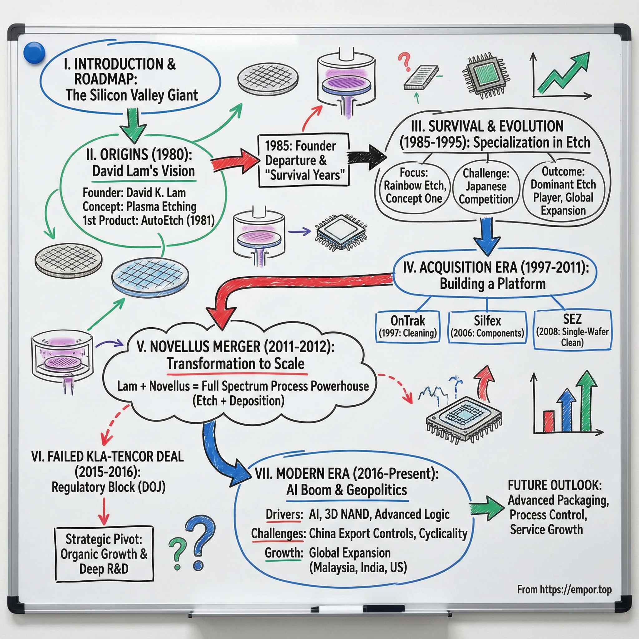
Lam Research: The Architects of the Atomic Sandbox
I. Introduction & Episode Roadmap [00:00 – 00:15]
Picture a structure thinner than a thousandth of a human hair, and now imagine carving a hole straight down through more than two hundred stacked layers of it — a hole so perfectly vertical that across its entire depth it must not bend or taper by more than the width of a few atoms. Do it billions of times, on a single wafer, in a few minutes, with essentially zero defects. If you cannot do that, the most advanced chip in the world is just an expensive piece of sand. The company that does it better than anyone else on Earth is Lam Research Corporation, traded on the Nasdaq under the ticker LRCX.1
Most investors who follow the semiconductor supply chain know the name ASML — the Dutch monopoly whose extreme ultraviolet lithography machines print the circuit patterns onto silicon. ASML gets the magazine covers because lithography is the photogenic part of chipmaking: light, lenses, the closest thing the industry has to a magic wand. But printing a design onto a wafer is, by itself, completely useless. A photograph of a skyscraper is not a skyscraper. Someone has to take that two-dimensional pattern and turn it into a real three-dimensional structure — adding microscopic layers of material atom by atom, then carving them away again with surgical precision. That is the unglamorous, brutally difficult half of the business called etch and deposition. And that is where Lam Research wins.
This is a company that in its fiscal third quarter ended in March 2026 generated $5.84 billion of revenue in a single ninety-day window — up roughly 24% from a year earlier — and that on an annual basis runs well above $18 billion.2 It supports an installed base of more than 100,000 process chambers humming inside fabs around the world.[^3] And here is the financial detail that should make any long-term investor sit up: since 2013, Lam has retired more than 60% of its outstanding shares, shrinking the pie so aggressively that each remaining slice has compounded even through brutal industry downturns.3
So how did a company founded by a Chinese-American physicist in a Santa Clara strip-mall-era startup become one of the three indispensable toll-collectors of the modern world? Here is the roadmap. First, the atomic founding concept — David Lam's bet that the entire industry was about to hit a wall. Second, the 2012 Novellus merger, one of the most disciplined acquisitions in technology history. Third, the 3D NAND vertical-scaling explosion that handed Lam a near-monopoly on the hardest etch on the planet. Fourth, the antitrust block of the KLA-Tencor mega-deal and the financial pivot it forced. Fifth, a clear-eyed look inside the two engines — the cyclical Systems business and the hidden services annuity called CSBG. And finally, the moats, the management, and the very real risks: geopolitics, memory cycles, and a competitor named Applied Materials that wants Lam's crown.
Let's start at the beginning, with a problem nobody could see but everybody was about to hit.
II. Founding Context & The Atomic Sandbox [00:15 – 00:30]
In 1980, in Santa Clara, California, a physicist named David K. Lam looked at how the semiconductor industry cleaned and shaped its silicon wafers and concluded that the whole approach was about to fail.1 At the time, the dominant method for carving patterns into a wafer was "wet etching" — and the name is exactly as literal as it sounds. Engineers would dunk a patterned wafer into a bath of liquid acid, and the acid would eat away the exposed material. For the chunky, generously-sized features of the 1970s, this worked fine.
But David Lam saw the trap. Acid is a liquid, and liquids do not respect direction. When you dip a wafer in acid to dig a trench, the acid eats downward, yes — but it also eats sideways, sneaking underneath the protective mask and widening the trench in every direction at once. Engineers call this "undercutting," and it is governed by surface tension, the same force that lets a water strider walk on a pond. At human scale, a little sideways erosion is invisible. But as chip features marched toward the sub-micron world — features smaller than a wavelength of visible light — that sideways creep was no longer a rounding error. It was the difference between a working chip and a smear. You cannot build a precise vertical wall by washing it with a liquid that flows everywhere.
David Lam's answer was to get rid of the liquid entirely. Instead of acid, use gas — but not ordinary gas. Energize it into plasma, the fourth state of matter, a glowing soup of charged particles. In a plasma etcher, you can grab those charged ions with an electric field and slam them straight down onto the wafer, like a billion microscopic jackhammers all striking perfectly vertically. Because you control the direction, you can carve a trench with near-vertical walls and almost no sideways undercutting. This is "dry plasma etching," and Lam's first product, the AutoEtch 480, was the industry's first single-wafer dry plasma etcher with computer control.1 The "single-wafer" detail mattered enormously: rather than batch-processing dozens of wafers at once and hoping they came out uniform, Lam's machine handled one wafer at a time under tight computer supervision, trading raw throughput for the precision and repeatability that smaller features demanded.
There is a tidy irony in the corporate history: David Lam himself departed the company in 1985, only five years after founding it, moving on to other ventures.1 He is not a part of the modern Lam Research story in any operational sense, and we will not pretend otherwise. But the technological DNA he stamped onto the company — single-wafer processing, computer control, and a deep mastery of plasma physics — turned out to be exactly the right foundation. Four decades later, the discipline of pushing ions one layer at a time has matured into "atomic layer etching," in which Lam's machines can remove material literally one atomic monolayer per cycle, and its mirror-image cousin atomic layer deposition, which adds material one monolayer at a time. The founder left early; the physics he bet on never did. And the next great chapter would come not from a single insight but from the realization that adding and removing material were becoming two halves of the same problem.
III. The Masterstroke M&A: Benchmarking the Novellus Acquisition [00:30 – 01:00]
By 2011, Lam had a problem that looked, on the surface, like success. It was the king of dry etch and a leader in wafer cleaning — genuinely excellent at removing material and washing wafers. But the semiconductor industry was crossing below the 20-nanometer threshold, and at that scale something strange was happening to the manufacturing process: the line between subtraction and addition was dissolving. To build a transistor at the leading edge, you no longer just deposited a layer and then etched it. You deposited an atomically thin film, etched part of it back, deposited again, etched again — a delicate back-and-forth choreography where the deposition step and the etch step had to be co-designed together or the whole structure failed. A company that could only etch was, increasingly, a company that could only see half the chessboard.
So Lam made the move that defined it. In December 2011, it announced the acquisition of Novellus Systems, a leading maker of deposition equipment — chemical vapor deposition and physical vapor deposition tools that add material to the wafer — in an all-stock deal valued at roughly $3.3 billion.4 Overnight, this would convert Lam from a one-handed etch specialist into an ambidextrous etch-and-deposition powerhouse that could co-optimize both halves of the new choreography.
Here is where the discipline of the deal deserves real scrutiny, because the price you pay determines whether even a strategically perfect acquisition creates or destroys value. Novellus had generated roughly $1.36 billion of revenue in its prior fiscal year. Lam's all-stock offer valued the company at an enterprise-value-to-revenue multiple of around 2.3x, with a premium to the undisturbed share price of roughly 28% — meaningful, but hardly euphoric.4 Now hold that up against the comparable transaction happening in the same industry at the same moment. Just months earlier, in May 2011, Applied Materials — Lam's largest rival — had agreed to acquire Varian Semiconductor for about $4.9 billion, a deal that worked out to something closer to 4.5x revenue and a premium north of 50%.5
The contrast tells you something durable about how Lam's leadership thinks. Applied Materials paid a steep, almost trophy-hunting multiple for scale; Lam paid a sober price for a capability it genuinely needed and could integrate. In a notoriously cyclical industry where acquirers routinely overpay at the top of the cycle and then write down the goodwill in the trough, avoiding the "winner's curse" is not a minor virtue — it is the whole game. The fact that the deal was all-stock also meant Lam was sharing the cyclical risk with Novellus's own shareholders rather than levering up the balance sheet to fund a cash purchase at a peak. With the benefit of hindsight, the Novellus acquisition stands as one of the most value-accretive transactions in the history of the semiconductor capital-equipment industry — not because Lam was lucky, but because it bought a real capability at a rational price and then actually integrated it.
And the deal carried a hidden asset that did not show up on the balance sheet: people. Novellus's then-chief operating officer was a Lam outsider named Timothy Archer, who was handed the job of executing the post-merger integration.6 Archer would not stay an integration manager for long. He would go on to run the entire combined company. The acquisition that gave Lam its second hand also, quietly, delivered its future chief executive. That combined etch-and-deposition platform was about to be tested by the single largest architectural shift the memory industry had ever attempted.
IV. Going Vertical: The 3D NAND Scaling Revolution [01:00 – 01:30]
Around 2013, the flash-memory industry walked into a wall it could not go through. Flash memory — the NAND that fills every phone, laptop, and data-center drive — had for decades gotten cheaper the same way the rest of the chip industry did: by shrinking. Pack the memory cells closer together on a flat, two-dimensional plane, and you get more storage per dollar. But by the time cell-to-cell spacing approached the mid-teens of nanometers, the physics rebelled. The cells were so close that electrons began to leak from one to its neighbor, quietly corrupting stored data. You cannot sell a storage product that forgets. Planar NAND had hit a hard physical limit.
The industry's escape was as audacious as it was simple to describe and fiendishly hard to build: if you cannot spread out, build up. Instead of cramming cells together on a flat plane, stack them vertically into towers — silicon skyscrapers. Memory makers led by 삼성전자 Samsung Electronics and SK하이닉스 SK Hynix pioneered this transition to "3D NAND," depositing dozens, and eventually well over two hundred, alternating layers of insulating and conducting films, one atop the next, like the floors of an impossibly tall building.1 Suddenly the bottleneck of the entire memory industry was no longer printing a fine pattern on a flat surface. It was a manufacturing challenge tailor-made for Lam.
Here is the killer step, and it is worth slowing down for. To make a 3D NAND tower actually function, you have to drill connecting channels straight down from the top of the stack to the bottom — through every single one of those two-hundred-plus layers in one shot. Return to the analogy from the open: imagine standing on the roof of the Empire State Building and drilling a hole all the way down to the basement, and demanding that the hole stay perfectly straight the entire way, never wandering, never tapering, never pinching shut, with a wall-to-wall tolerance measured in atoms. This is "high-aspect-ratio dielectric etch" — "high aspect ratio" being engineer-speak for "very deep and very narrow." It is arguably the single most difficult routine operation in all of semiconductor manufacturing, and it is precisely the discipline that Lam's mastery of plasma physics and high-power radio-frequency ion acceleration was built for. On the most critical channel-hole etch steps in 3D NAND, Lam came to hold a market position that approached effectively total dominance — a near-monopoly on the hardest hole in the world.[^3]
The financial consequence was a multi-year surge in Lam's systems revenue, but the strategic consequence mattered more. The vertical transition cemented Lam as an indispensable partner to the memory industry, not a swappable vendor. When the hardest step in your entire production line works only because of one company's chambers, that company stops being a supplier and becomes a dependency. That dependency would prove to be both Lam's greatest strength and, as we will see, the source of its single greatest vulnerability — because memory is the most violently cyclical corner of an already cyclical industry. But before that vulnerability bit, Lam's leadership tried to make one more enormous move, and the U.S. government stopped them cold.
V. The DOJ Pivot: The Blocked KLA-Tencor Deal & The Shareholder Return Engine [01:30 – 01:55]
In October 2015, flush with the success of the Novellus integration and the 3D NAND boom, Lam swung for the fences. It announced an agreement to acquire KLA-Tencor — the undisputed global leader in semiconductor metrology and inspection — in a cash-and-stock deal valued at roughly $10.6 billion.[^8] The strategic logic was seductive. Etch and deposition shape the wafer; metrology and inspection measure it and hunt for defects. Owning both would have given Lam a consolidated process-and-measurement platform of staggering breadth, the kind of vertically integrated giant that could, in theory, optimize the entire manufacturing flow under one roof.
That breadth was exactly the problem. The U.S. Department of Justice's Antitrust Division, coordinating with regulators around the world, took a hard look and saw a threat to competition. KLA's inspection tools are the referees of the fab — the instruments that detect the microscopic defects produced by everyone's equipment, including Lam's competitors. The fear, in antitrust language, was "vertical foreclosure": if Lam owned the referee, it could quietly tune KLA's tools to flatter its own etch and deposition chambers and disadvantage rivals like 東京エレクトロン Tokyo Electron and Applied Materials, who depend on KLA's instruments to qualify their own machines. In October 2016, facing that resistance, Lam and KLA-Tencor abandoned the merger.[^8] Crucially, the termination was clean — no breakup fee changed hands.[^8] The deal simply evaporated, and Lam walked away with its capital intact but its grand consolidation strategy in ruins.
What management did next is, for long-term investors, the most revealing decision in the company's modern history. Blocked from buying growth through mega-M&A, Lam's leadership — increasingly shaped by chief financial officer Doug Bettinger — did not go hunting for some other empire to build. Instead, it pivoted hard toward returning capital and funding its own research. Over the following years this crystallized into an explicit capital-return philosophy: commit to returning the lion's share of free cash flow to shareholders, year in and year out, while protecting the research budget that feeds the next technology node.3
The mechanics of that pivot have been remarkable, and the numbers tell a story of relentless compression. The reason Lam has retired more than 60% of its share count since 2013 is precisely this post-KLA discipline: rather than letting cash pile up or chasing splashy acquisitions, management used the cyclical downturns — when the stock was cheap and pessimism was high — to buy back stock aggressively, turning the industry's volatility into a friend.3 In May 2024, the board underscored the commitment with a fresh $10 billion share-repurchase authorization, and in the same breath announced a 10-for-1 stock split to keep the shares accessible to a broader base of investors.78 The analytical takeaway is straightforward: a company that buys its own shares hardest when its industry is most hated, and that funds those buybacks from genuine free cash flow rather than debt, is signaling real confidence in the durability of its cash generation. Whether that confidence is justified depends entirely on the two engines that actually produce the cash — and those engines deserve a close look.
VI. Core Engine I: Systems Segment & The WFE War [01:55 – 02:35]
Walk onto the floor of a leading-edge fab and the Lam machines you see — the big, humming etch and deposition chambers being installed for the first time — are the Systems business. This is the segment that sells new equipment, and it is the larger of Lam's two engines, accounting for somewhere in the low-to-mid sixties as a percentage of total revenue.2 It is also the more glamorous and the more brutally cyclical: when chipmakers are confident, they pour tens of billions into new fabs and Systems revenue soars; when they lose their nerve, they slam the brakes and Systems revenue can fall off a cliff in a single year. This is the front line of what the industry calls the WFE war — WFE being "wafer fab equipment," the roughly $140 billion global market that Lam, in its April 2026 outlook, forecast for the calendar year on the back of accelerating artificial-intelligence demand.2
The competitive structure of this market is best understood not as a free-for-all but as a tightly segmented oligopoly. In dry etch — Lam's ancestral home — Lam holds the leading global position, with roughly 45% of the market, ahead of Applied Materials at around a third and 東京エレクトロン Tokyo Electron at roughly 15%.[^3] In the broader deposition market the picture flips: Applied Materials is the scale leader across the widest range of chemical and physical deposition, while Lam, drawing on its Novellus inheritance, has carved out highly profitable specialist leadership in atomic layer deposition and plasma-enhanced chemical vapor deposition. The point is that these three players rarely compete on price across the whole board; instead they fight ferociously, fab by fab and step by step, for a designation that is the true prize of this industry: "Tool of Record."
To understand why Tool of Record is everything, you have to understand co-optimization. When a chipmaker develops a brand-new architecture — a next-generation logic transistor or a new flavor of high-bandwidth memory — it does not buy equipment off a shelf. It works hand-in-glove with vendors to develop a "recipe," a precisely tuned sequence of process steps. Lam's structural edge here is that it can deposit a single monolayer of atoms and then immediately etch that monolayer back, all on one integrated platform, eliminating the defect-inducing delays that occur when a wafer has to be shuttled between different machines from different vendors. Once a customer qualifies that integrated recipe for high-volume manufacturing, the chamber that ran it becomes the Tool of Record for that step — and the switching cost becomes, for practical purposes, prohibitive. Swapping in a competitor's tool would mean re-characterizing the entire chemical process and risking yield, and in this industry a yield drop of even a single percentage point can vaporize a fab's economics. We will return to the depth of that moat later; for now, simply note that winning Tool of Record at a new node is like being written into the genetic code of a product line for its entire commercial life.
So where is the money actually flowing today? Two transitions matter most. The first is the move in leading-edge logic away from the FinFET transistor toward "gate-all-around" nanosheet structures — a change in the fundamental shape of the transistor that opens up fresh battles over which vendor's tools win the critical new steps. Lam has concentrated on the steps where its physics gives it an edge, particularly the exquisitely selective etch that removes sacrificial silicon-germanium layers without so much as scratching the adjacent silicon channels, and the deposition of the "inner spacer" that insulates the structure. The honest framing, though, is that this is contested ground: Applied Materials is pushing hard to integrate these very steps into its own platforms, and the GAA transition is precisely where Lam's logic moat is most exposed to attack — a thread we pick up in the bear case. The second transition is in memory: the explosion of high-bandwidth memory for AI accelerators, where HBM3e and HBM4 require deep through-silicon vias — vertical tunnels drilled through the DRAM dies so they can be stacked — which demands exactly the kind of intense, high-aspect-ratio dielectric etch that is Lam's signature strength. AI, in other words, is not an abstraction for Lam; it shows up as physical demand for the hardest holes in the industry. But the new-equipment engine is only half the story, and arguably not the half that keeps the company stable through the cycle.
VII. Core Engine II: The CSBG Annuity — Lam's Hidden $7 Billion Buffer [02:35 – 03:05]
Here is the part of Lam Research that almost nobody outside the industry talks about, and it may be the most important part of the entire investment case. Every one of those 100,000-plus chambers Lam has sold over the decades does not just sit in a fab running forever for free. It needs spare parts — proprietary ones. It needs maintenance. It needs upgrades, refurbishment, and software. And the business that supplies all of that is the Customer Support Business Group, or CSBG, which accounts for roughly the high-thirties as a percentage of Lam's revenue and runs at an annual scale around $7 billion.2 It is, in effect, a vast hidden annuity bolted onto the back of the cyclical hardware business.
The scale finally became impossible to ignore in early 2026. In the March 2026 quarter, CSBG crossed $2 billion in quarterly revenue for the first time in the company's history, a milestone management attributed to high fab utilization and newer service offerings, including its Equipment Intelligence software and a line of "Dextro" service cobots.2 To grasp why this matters, you have to understand how CSBG revenue behaves differently from Systems revenue. The Systems business is tied to capital expenditure — to chipmakers' decisions about whether to build new fabs, decisions that swing wildly with sentiment and the memory cycle. CSBG, by contrast, is tied to "wafer starts" and tool utilization: as long as a fab is physically running wafers through Lam's installed chambers, the operator has no choice but to keep buying high-margin proprietary spare parts and paying for service, regardless of whether anyone is building new fabs that year.
That distinction is the difference between a business that whipsaws and a business that hums. When the capital-expenditure cycle turns down and Systems revenue contracts, fabs do not switch off their existing tools — they often run them harder, milking the installed base, which keeps CSBG revenue resilient and its cash flowing. The segment's margins reinforce the point: services and proprietary spares carry structurally higher and far more stable profitability than selling new systems, which is exactly what you want from a counter-cyclical cushion. The independent, skeptical read is that this is the single most underappreciated asset on Lam's income statement — a recurring, utilization-linked, software-like cash engine hiding inside what looks from the outside like a pure capital-equipment cyclical.
There is also a strategic option embedded here. When a customer cannot justify the staggering cost of an entirely new fab, it can instead turn to CSBG to upgrade its existing tools — installing new chambers, gas manifolds, and software to squeeze more capability out of equipment it already owns. At its 2025 Investor Day, management set a target of growing CSBG by roughly 1.5x by 2028, with longer-term ambitions to double it as the broader industry marches toward $1 trillion in annual revenue, and framed the whole effort as a core value driver rather than an afterthought.9 The appropriate posture toward that target is constructive skepticism: an installed base of this size makes the growth mathematically plausible, but a target is a promise, not a result, and investors should track CSBG's actual quarterly trajectory against it. That same Investor Day also unveiled a set of ambitious bets on the future — and one of them could reshape Lam's addressable market entirely.
VIII. Future Bets & Speculative Novelties: Dry Resist EUV [03:05 – 03:20]
It is worth being honest up front about proportion: the technology in this section generates a rounding error of Lam's revenue today, and it earns its place not because of what it contributes now but because of the size of the door it could open later. The bet is called dry resist, and it lives at the boundary between Lam's world and ASML's.
Here is the problem it attacks. Lithography needs a "photoresist" — a light-sensitive coating spread across the wafer that hardens or softens where the light hits, forming the pattern that subsequent steps carve into the silicon. For decades that resist has been applied as a liquid, spun onto the wafer in a thin film, the way you might pour batter onto a griddle and tilt it to spread. But as features shrink below 30 nanometers and the industry moves to ever-finer extreme-ultraviolet patterning, that liquid film starts to betray its physics. The same surface tension that doomed wet etching four decades ago returns to haunt the resist: the tall, ultra-thin patterned structures can literally collapse like wet sandcastles, producing ragged line edges and defects.
Lam's answer, developed in collaboration with ASML and the Belgian research institute IMEC, is to do to the resist what David Lam did to etching all those years ago — get rid of the liquid.10 Instead of spinning on a liquid resist, Lam uses chemical vapor deposition to grow a dry, metal-oxide photoresist directly onto the wafer from a gas phase, and then uses a dry plasma process to develop it.10 It is a conceptually elegant move: the same gas-phase, plasma-centric expertise that defines Lam's core business, applied to a step that has always belonged to the wet-chemistry world.
The investment significance is pure optionality. If dry resist is adopted widely by leading-edge foundries running High-NA EUV, Lam would gain a high-margin foothold in the patterning stream — a part of the manufacturing flow historically dominated by Japanese specialty-chemical giants such as 東京応化工業 Tokyo Ohka Kogyo and JSR. That would expand Lam's serviceable market beyond its traditional etch-and-deposition turf into lithography-adjacent territory. The honest caveat is that adoption is not assured, timelines in this industry routinely slip, and incumbents do not surrender lucrative steps quietly. Dry resist is a real call option with a real strike price — valuable, but not yet in the money. Whether bets like this pay off ultimately comes down to the people allocating the capital and setting the priorities.
IX. Modern Stewardship: Leadership Credibility, Incentives, & Alignment [03:20 – 03:40]
The two people who matter most to the modern Lam Research story are the chief executive, Timothy Archer, and the chief financial officer, Doug Bettinger. Archer, as we have seen, arrived through the Novellus acquisition as that company's chief operating officer and was first handed the unglamorous job of stitching the two organizations together before eventually rising to the top job.6 That trajectory matters: he is an operator who earned the corner office by integrating an acquisition rather than a financier parachuted in to dress up a balance sheet. Bettinger, for his part, has been the architect of the capital-allocation discipline that defines the post-KLA era — the steady hand on the buyback lever.
For long-term investors, the right way to judge management is not by the polish of its slides but by the alignment of its incentives and the consistency of its behavior over time. On alignment, the picture is encouraging. Archer holds well over a million shares directly — a personal stake worth several hundred million dollars in the 2025–2026 trading bands — meaning his own net worth rises and falls with the same shares that ordinary holders own.11 His compensation is overwhelmingly at-risk rather than guaranteed salary, and a majority of his long-term incentive award is delivered as performance shares that pay out based on Lam's total shareholder return measured relative to a peer index.11 That last detail is the one that counts: tying a CEO's biggest pay component to relative shareholder return means he is rewarded for beating his industry, not merely for riding a cyclical updraft that lifts every semiconductor stock at once.
A skeptic will reasonably flag the insider selling. In December 2025, Archer sold a block of stock — on the order of 163,000 shares — under a pre-arranged Rule 10b5-1 trading plan.11 It is worth explaining to non-specialists why this is, in itself, not a red flag. A 10b5-1 plan is a schedule set up in advance, at a time when the executive has no inside information, that then executes automatically on preset dates regardless of news; it is the standard, legally-sanctioned mechanism executives use to diversify concentrated wealth and handle estate planning without the appearance of trading on secrets. The presence of such sales is normal; what would be alarming is a pattern of executives tearing up plans and dumping stock ahead of bad news, and there is no evidence of that here.
The more demanding test of credibility is behavior under stress and the absence of empire-building. On the first count, since the blocked KLA deal Lam has conspicuously avoided dilutive mega-mergers, sticking instead to small, high-return technology tuck-ins — the 2017 purchase of the modeling-software company Coventor and the 2023 acquisition of the advanced-packaging wet-processing specialist SEMSYSCO are representative of the type.1 That is discipline consistent with the post-2016 promise. On the second count, the 2023 memory downturn offered a live test of transparency: when memory capital spending collapsed, management did not paper over the decline. It guided revenue down candidly, executed targeted structural cost reductions while protecting the research budget, and leaned into the depressed share price to accelerate buybacks — the same counter-cyclical reflex described earlier, now demonstrated in a real downturn rather than promised in a slide. The narrative held together across calls and filings, which is itself a form of credibility. None of this guarantees the future, but it establishes a track record worth weighing against the durable advantages we turn to next.
X. Playbook: Strategic Moats (Hamilton's 7 Powers & Porter's 5 Forces) [03:40 – 04:05]
Strip away the engineering and the question for an investor is simple: what stops a competitor from taking Lam's business? Two frameworks help organize the answer — Hamilton Helmer's 7 Powers and Michael Porter's Five Forces — and Lam scores genuinely well on both, with important caveats.
Start with the powers. The primary and most durable is switching costs, the mechanism introduced when we discussed Tool of Record. Once a chemical recipe and chamber configuration are qualified for high-volume manufacturing at a given node, replacing that tool with a rival's would force the customer to re-characterize the entire process and gamble with yield — and because a yield drop of even one percentage point can wreck a fab's economics, the incumbent tool is effectively irreplaceable for the commercial life of that node. This is not a soft, brand-loyalty switching cost; it is a hard, physics-and-economics switching cost, which is the most valuable kind. The second power is a cornered resource: Lam's deep patent library and accumulated process know-how in high-aspect-ratio etch, dry development, and atomic-layer etching represent decades of plasma-physics learning that cannot simply be hired or reverse-engineered overnight. The third is scale economies, most visible in research and support: Lam spends on the order of $2 billion-plus a year on research and development, and maintains a global service infrastructure capable of keeping 100,000-plus tools running around the clock — a fixed-cost base that a new entrant could not hope to replicate or justify against a standing start.[^3]
Now Porter's Five Forces, which sharpen where Lam is strong and where it is exposed. The bargaining power of buyers is very high, and this is the genuine pressure point: Lam's customer base is extraordinarily concentrated among a handful of giants — 台積電 TSMC, Samsung Electronics, Intel, SK Hynix, and Micron — who control the overwhelming majority of global WFE spending and use that leverage to extract steep discounts, bespoke customization, and absolute support. When five customers are most of your market, they have you on a short leash, and that caps Lam's pricing power even where its technology is dominant. By contrast, the threat of new entrants is for all practical purposes zero — the combined technological, financial, and relationship barriers are simply insurmountable for a newcomer. The bargaining power of suppliers sits in the low-to-moderate range: Lam relies on highly specialized component makers, but its own scale gives it dominant purchasing leverage over most of them. And competitive rivalry is high but rational — a segmented oligopoly in which Lam, Applied Materials, and Tokyo Electron wage disciplined, step-by-step combat for Tool of Record at each new node rather than ruinous across-the-board price wars.
The synthesized verdict is that Lam's moat is real, deep, and grounded in hard switching costs and irreproducible scale — but it is not unconditional. It is strongest precisely where Lam already won the last node, and it must be re-won at every architectural inflection, against well-funded rivals, in front of customers powerful enough to play vendors against one another. A moat that has to be re-dug at every transition is a good moat, but it is not a sleepy one. And the places where it is thinnest are exactly where the bears train their fire.
XI. The Bear Case & Risk Radar: Activist/Skeptic Stress Test [04:05 – 04:30]
Imagine a skeptical hedge fund manager building a short position in Lam, or an activist taking a stake to agitate. What would they hammer on? Two structural arguments, and two acute risks.
The first structural argument is what we might call the China trap. In recent years China has been an enormous slice of Lam's revenue — running in the mid-thirties as a percentage of the total, driven by a domestic boom in mature-node, or "legacy," chip manufacturing as Chinese firms raced to build out capacity insulated from sanctions.2 The bear's question is pointed: is that demand real and durable, or is it a pull-forward — a one-time stockpiling surge that will collapse once China either achieves equipment self-sufficiency or simply finishes building the fabs it was always going to build? The early evidence gives the bear some ammunition, because China's share has already begun to recede: in the March 2026 quarter it dipped to 34% and management explicitly guided it lower, with Korea and Taiwan rising to take its place.2 A declining China mix can be read two ways — as healthy diversification toward leading-edge demand, or as the leading edge of a feared rollover. Both readings are live.
The second structural argument is the memory-concentration penalty. Lam's stock has historically traded at a valuation discount to ASML, and the reason is structural: Lam carries heavier exposure to the violently cyclical memory market, especially NAND, than its more logic-weighted peer. When the memory cycle turns down, Lam's Systems growth lags, and the market prices that volatility as a permanent discount. An activist would argue that until Lam can durably diversify away from memory's mood swings, it will wear that discount no matter how well it executes. The counter is the CSBG annuity and the AI-driven HBM and logic demand discussed earlier — but the bear would note those are precisely the things management is asking investors to take partly on faith.
Then there are the two acute risks on the radar. The first is geopolitical export control. Lam's largest geographic market is also the one most exposed to the stroke of a regulator's pen: should the U.S. government tighten restrictions on selling even legacy-node deposition and etch equipment into China, a material chunk of revenue could disappear overnight, with little Lam could do about it. This is not a hypothetical tail risk; it is an active, evolving policy environment, and it is the single cleanest way the bull thesis could break. The second acute risk is the architecture transition we flagged earlier: the gate-all-around land grab in leading-edge logic. Applied Materials is aggressively marketing integrated materials-engineering platforms and claiming share gains at exactly this inflection; if it succeeds in folding the critical selective-etch step directly into its own deposition chambers, it could breach Lam's etch moat in logic at the very moment that moat is being re-dug. The honest assessment is that Lam's defenses here are strong but not proven for the full GAA ramp, and this is the competitive battle most worth watching. Weighing all of it together is the work of the final section.
XII. Epilogue & Key Takeaways [04:30 – 04:45]
Step back from the plasma physics and the proxy statements, and what is Lam Research, really? It is a toll-booth — one of perhaps three in the world — on the road to every sub-2-nanometer transistor and every vertically-stacked memory tower humanity will build. It is not merely a hardware cyclical to be traded around the WFE cycle, though it is partly that; it is the holder of a hard, physics-grounded position at the precise step where the most advanced chips are most likely to fail without it. That position is genuinely valuable. It is also, as we have seen, conditional, contested, and exposed to forces — the memory cycle, Beijing, Washington, and a rival named Applied Materials — that no amount of execution can fully control.
Three business lessons endure from the story. The first is acquisition discipline: the Novellus deal worked not because it was big but because Lam bought a capability it truly needed, at a rational multiple, and kept the talent — including a future CEO — rather than overpaying for trophy scale the way its larger rival did with Varian. The second is the pivot moat: when the government blocked Lam's path to growth-by-consolidation in the KLA-Tencor deal, management did not sulk or scheme for the next empire; it pivoted instantly to structural capital returns and compounded shareholder value by retiring a majority of its shares through the cycle. The third is the hidden annuity: a massive physical installed base, properly serviced, becomes a recurring, software-like cash engine that stabilizes an otherwise volatile enterprise — the CSBG lesson that the market still under-weights.
What should a long-term investor actually watch from here? Two or three KPIs cut through the noise. Watch CSBG revenue and its trajectory against management's 1.5x-by-2028 target — it is the single best gauge of whether the counter-cyclical annuity is real and growing as promised.9 Watch the China revenue mix — it is the cleanest barometer of both geopolitical risk and the durability of the recent demand surge.2 And watch Tool-of-Record outcomes at the gate-all-around logic transition — the place where Lam's most important moat will either hold or be breached. Lam Research has spent four decades proving it can carve the impossible hole. The open question, as always in this industry, is whether it can keep winning the next node before the cycle, the geopolitics, or the competition carves into it first.
References
-
Lam Research Corporation — Reuters Company Profile, NASDAQ:LRCX Core Metrics ↩↩↩↩↩↩
-
Lam Research (LRCX) Q3 2026 Earnings Transcript — The Motley Fool, 2026-04-22 ↩↩↩↩↩↩↩↩
-
Lam Research Corporation Announces $10 Billion Share Repurchase Authorization — Lam Research Newsroom, 2024-05-21 ↩↩↩
-
Lam Research Agrees to Acquire Novellus Systems for $3.3 Billion in Stock — Reuters, 2011-12-14 ↩↩
-
Applied Materials Agrees to Acquire Varian Semiconductor for $4.9 Billion — Bloomberg, 2011-05-17 ↩
-
SEC EDGAR — Lam Research Corporation Filings (CIK 0000707549) ↩↩
-
Lam Research Q3 Fiscal Year 2026 Quarterly Financial Results — Lam Research Newsroom, 2026-04-22 ↩
-
Lam Research Corporation Announces 10-for-1 Stock Split — Lam Research Newsroom, 2024-05-21 ↩
-
Lam Research: We Raise Our Valuation After Upbeat Investor Day, but See 2028 Targets as Optimistic — Morningstar, 2025-02 ↩↩
-
Lam Research Announces Breakthrough EUV Dry Resist Technology — Lam Research Newsroom, 2020-03-03 ↩↩
-
Lam Research Corporation — SEC EDGAR Proxy Statement (DEF 14A) and Insider Transaction Filings ↩↩↩
 RSS Feed
 Spotify
 Apple Podcasts
 Amazon Music
 Audible
 YouTube