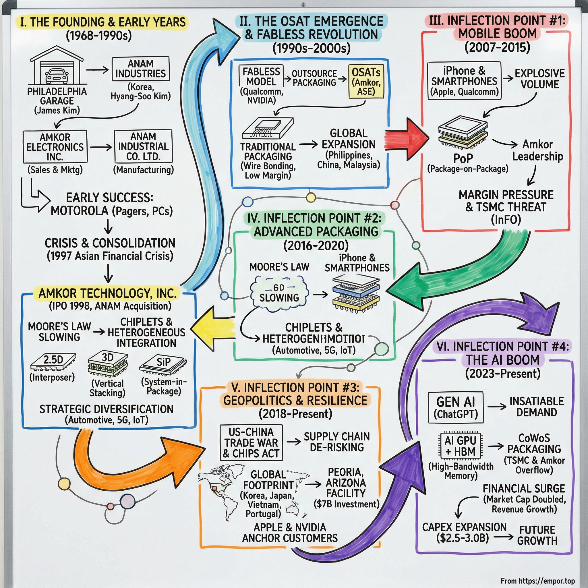
Amkor Technology: The Hidden Giant of the Semiconductor World
I. Introduction & Episode Roadmap
Here is a question that reveals a blind spot in how most people think about technology: who packages the chips?
Not who designs them — that would be Apple, NVIDIA, Qualcomm, AMD. Not who fabricates them — that would be TSMC, Samsung, Intel. But who takes the raw silicon that comes off a fabrication line and turns it into a finished product that can actually be put inside a phone, a server, or a car? The answer, for a staggering percentage of the world's semiconductors, is a company that most people have never heard of.
Somewhere inside the phone in your pocket, the laptop on your desk, and the GPU humming inside a data center training an AI model, there is a chip that was packaged by that company. That company is Amkor Technology, the world's second-largest outsourced semiconductor assembly and test provider, and one of the most consequential businesses operating in the shadows of the semiconductor supply chain.
Amkor does not design chips. It does not fabricate them. What it does is take the raw silicon dice that come off a foundry's production line and turn them into finished, usable products — encasing them in protective packages, wiring them to circuit boards, stacking memory on top of processors, and testing every single unit before it ships. If TSMC is the chef who cooks the meal, Amkor is the one who plates it, garnishes it, and makes sure it does not poison anyone. That analogy undersells the complexity. Modern advanced packaging is arguably as technically demanding as the fabrication itself, involving nanometer-scale interconnects, three-dimensional stacking, and materials science that pushes the boundaries of physics.
Why does Amkor matter right now? Three forces have converged to make this formerly obscure company suddenly strategic. First, the AI boom has created an insatiable demand for advanced packaging — the same kind of packaging that Amkor specializes in. The bottleneck in building AI chips is no longer just fabrication capacity at TSMC; it is the ability to package those chips with high-bandwidth memory using technologies like CoWoS, fan-out, and 2.5D integration. Second, geopolitics has reshuffled the deck. The U.S.-China trade war and the CHIPS Act have made domestic semiconductor manufacturing a national security priority, and Amkor is building the largest outsourced advanced packaging facility in the United States in Peoria, Arizona. Third, the economics of chipmaking have fundamentally shifted. As Moore's Law slows and chiplet-based architectures emerge, packaging has gone from being the "boring back end" to the critical enabler of next-generation performance.
The numbers tell part of the story. Amkor's market capitalization has nearly doubled in just over a year, from roughly $6.3 billion in January 2025 to approximately $12 billion by February 2026. Its 2026 capital expenditure plan of $2.5-3.0 billion is nearly three times what it spent in 2025. The company broke ground on a $7 billion Arizona campus that will be the largest outsourced advanced packaging facility in the United States, with Apple and NVIDIA as anchor customers.
But the real story is not the numbers — it is the question of whether a company that spent decades as a low-margin, commodity manufacturer has genuinely transformed into something strategically indispensable. How did a Korean family business founded in a Philadelphia garage become critical infrastructure for the global semiconductor industry? Why did packaging — historically the lowest-margin, most commoditized part of chipmaking — suddenly become strategic? And can Amkor transcend its commodity origins to become something more durable?
II. Semiconductor Context: Why Packaging Matters
To understand why Amkor matters, you first need to understand what semiconductor packaging actually is, why it exists, and why it was ignored for so long. This requires a brief but important detour into the physics and economics of chipmaking — the kind of context that separates a superficial stock analysis from a genuine understanding of the business.
The semiconductor value chain has four major stages. First, a chip is designed — companies like Apple, NVIDIA, and Qualcomm employ thousands of engineers to architect the circuits that will eventually be etched into silicon. Second, that design is fabricated — this is the domain of foundries like TSMC, Samsung, and Intel, which operate the most expensive factories on Earth to print transistors measured in nanometers. Third, the fabricated silicon must be packaged — cut from the wafer, connected to external circuits, encased in a protective shell, and made ready for use. Fourth, every packaged chip must be tested to ensure it works.
For decades, the third step was treated as an afterthought. Fabrication was where the magic happened, where billions of transistors were etched using extreme ultraviolet lithography onto wafers of crystalline silicon. Design was where the genius lay — the architects who conceived of a processor's logic. Packaging? That was just putting the chip in a box. The analogy people used was that fabrication was like building a skyscraper, while packaging was like putting it in a shipping container.
This perception was not entirely wrong in the early days. Traditional packaging involved relatively straightforward processes: a die was placed on a lead frame, thin gold or copper wires were bonded from the die's contact pads to the frame's leads, and the whole thing was encapsulated in epoxy resin. This is wire bonding, and it remains the most common packaging technique for simple, low-pin-count devices. It is cost-effective, well-understood, and frankly not very exciting.
The margins reflected this simplicity. Traditional packaging was a low-value-add operation — the materials were cheap, the equipment was relatively affordable, and the labor could be trained in weeks rather than years. This is why packaging factories migrated to low-cost Asian locations in the 1960s and 1970s, following the same logic that sent textile manufacturing overseas.
But the demands of modern electronics shattered this simplicity. As chips grew more complex, they needed more connections to the outside world — more input/output pins, faster data rates, better thermal management. The industry moved from wire bonding to flip chip technology, where the die is flipped upside down and connected to the substrate through tiny solder bumps on its active face. This shortened the electrical path, improved performance, and allowed higher I/O density. Think of it as going from plugging in a lamp with a single cord to connecting a server rack with hundreds of fiber optic cables — the physical interface itself became a performance bottleneck.
Then came system-in-package, where multiple dies — a processor, memory, sensors, radio frequency components — were integrated into a single package. And then 2.5D packaging, where chips are placed side by side on a silicon interposer, a kind of high-speed highway that routes signals between them. And now 3D packaging, where dies are literally stacked on top of each other, connected through vertical tunnels called through-silicon vias. Each generation made packaging more complex, more capital-intensive, and more critical to the final product's performance.
Why did chipmakers outsource this work instead of doing it themselves? The same reason they outsourced fabrication: economics. Packaging requires specialized equipment, cleanroom facilities, and process expertise. But unlike fabrication, where a single leading-edge fab costs $20 billion or more, packaging facilities are cheaper to build — a few hundred million to a couple billion dollars — and the technology changes on a different cadence. For an integrated device manufacturer like Intel or Texas Instruments, running a packaging operation alongside a fab made sense when volumes were high. But as the industry fragmented and fabless companies proliferated, a new model emerged: let specialists handle it.
The economics are worth pausing on, because they explain why the OSAT industry exists at all. A packaging line might cost $200-500 million to build and equip. That is serious money, but nothing compared to a $20 billion fab. The catch is that a packaging line needs high utilization to be profitable — running three shifts, processing thousands of units per hour, with yield rates above 99 percent. A single company's chip volumes might not justify a dedicated packaging line. But an OSAT serving dozens of customers can keep that line running at full capacity, spreading the fixed costs across a much larger revenue base. This is the classic economics of specialization: the specialist who serves many customers can invest more, achieve better yields, and offer lower prices than the generalist who serves only itself.
The OSAT model also offered flexibility. A fabless company launching a new chip could start with low volumes during product qualification, ramp to millions of units per month during peak demand, and wind down gracefully at end of life — all without owning a single piece of packaging equipment. The OSAT absorbed the capital risk and demand volatility, earning a modest margin in exchange for providing elastic capacity. It was not a glamorous business, but it was a necessary one. And that is how Amkor found its niche.
III. Founding Story & The Kim Family Legacy (1968–1990s)
Every great technology company has a founding myth. Apple has the garage in Los Altos. TSMC has Morris Chang's flight from Texas Instruments. Amkor's myth is perhaps the most improbable of all: it begins not in Silicon Valley but in postwar Korea, and not with a technologist but with a bicycle importer. In 1935, Hyang-Soo Kim established ANAM Industries in Seoul, originally a trading company importing Japanese goods including bicycles. It was a modest enterprise in a devastated country, but Hyang-Soo had an instinct for where the world was heading. By the 1960s, as South Korea's government embarked on an aggressive industrialization strategy, he recognized that electronics manufacturing would be central to the country's economic future.
In March 1968, ANAM Industries was reorganized into ANAM Industrial Co. Ltd. and pivoted into semiconductor assembly. The operation was tiny by any standard: three wire bonders and two die bonders in a factory in Seoul. But the timing was impeccable. American semiconductor companies — Fairchild, Motorola, Texas Instruments — were looking for low-cost assembly partners in Asia to handle the labor-intensive work of packaging. Korea, with its disciplined workforce, government support for export industries, and proximity to Japan's electronics ecosystem, was an ideal location. By 1970, ANAM achieved a milestone that would echo through Korean industrial history: the country's first semiconductor export, shipping packaged chips in metal cans to the United States.
Meanwhile, Hyang-Soo's eldest son, James Kim — born Joo-Jin Kim in Seoul in 1936 — had taken a very different path. At nineteen, he immigrated to the United States in 1955, spent a year in Colorado learning English, and then enrolled at the Wharton School at the University of Pennsylvania. He earned both a bachelor's degree and a master's in economics, then became a professor at Villanova University. James Kim was an academic who happened to come from a family that made things, and that combination — analytical rigor married to manufacturing pragmatism — would define Amkor's culture for decades.
In April 1968, just one month after ANAM Industrial's semiconductor pivot, James Kim founded Amkor Electronics Inc. from an office in his garage in Philadelphia. The name was a portmanteau of "America" and "Korea," and it perfectly described the company's model: James would handle sales, marketing, and customer relationships in the United States, while ANAM would handle manufacturing in Korea. Though legally separate entities — structured that way for tax and regulatory purposes — the two companies operated as a single organism. James Kim was the face to Western customers, translating Korean manufacturing capability into American contracts.
The relationship with Motorola proved foundational. As one of the largest semiconductor companies in the world during the 1970s and 1980s, Motorola needed massive packaging capacity for its microprocessors, memory chips, and automotive semiconductors. ANAM became a trusted subcontractor, and James Kim's Wharton pedigree and American citizenship gave Motorola's executives confidence that they were dealing with a partner who understood Western business practices. It was a pattern that would repeat — Amkor serving as the bridge between Asian manufacturing and American technology companies.
Through the 1970s and 1980s, ANAM grew alongside Korea's semiconductor ambitions. The Korean government, through a combination of subsidies, protective tariffs, and strategic planning, was building a semiconductor industry that would eventually produce Samsung and SK Hynix. Korea's approach was distinctive: the government identified semiconductors as a strategic industry, funneled capital toward it through state-directed lending, and protected domestic companies while demanding they become globally competitive. This was the same playbook that built Korea's steel, shipbuilding, and automotive industries, and it worked spectacularly for semiconductors. ANAM was not a chaebol on the scale of Samsung or Hyundai, but it benefited from the same ecosystem: educated engineers graduating from Korea's rapidly expanding university system, government support for exports, and a national culture that valued manufacturing excellence and relentless improvement.
It is worth noting just how remarkable this trajectory was. In the span of a single generation, a family that had started by importing bicycles had become a critical supplier to the American semiconductor industry. ANAM's factories in Korea were packaging chips that went into Motorola's pagers, into early personal computers, into military electronics. The speed of this transformation mirrors the broader Korean economic miracle — a nation that went from postwar devastation to industrial powerhouse in thirty years.
The Amkor-ANAM model also reflected something deeper about the Korean-American diaspora in the technology industry. James Kim operated in two worlds simultaneously — the formal, contract-driven business culture of American semiconductor companies and the relationship-oriented, family-centric Korean industrial ecosystem. He could sit across the table from a Motorola purchasing executive and speak the language of quality metrics and delivery schedules, then fly to Seoul and navigate the personal relationships that drove Korean business. This bicultural fluency was a genuine competitive advantage at a time when cross-Pacific supply chains were novel and trust was hard to build.
By the early 1990s, ANAM had grown into one of the largest semiconductor packaging operations in the world, with multiple factories in Korea and a workforce of thousands. But the two-company structure — Amkor handling sales in America, ANAM handling manufacturing in Korea — was becoming increasingly unwieldy. Transfer pricing disputes, governance complexity, and the challenge of coordinating strategy across two legally separate entities created friction that grew as the business scaled.
The critical inflection came in the 1990s, driven by crisis. The 1997 Asian financial crisis devastated Korea's economy. The won collapsed, conglomerates defaulted on debt, and the entire industrial structure was forced to restructure. For ANAM and Amkor, the crisis accelerated a separation that had been building for years. James Kim moved to formally acquire ANAM's packaging operations, consolidating the business under the Amkor umbrella. In the second quarter of 1999, Amkor agreed to purchase a stake in ANAM worth $150 million. Then, in early 2000, Amkor paid $1.4 billion to acquire ANAM's three remaining packaging and test factories.
The timing of the IPO — May 1, 1998, on NASDAQ at approximately $13.31 per share — was both bold and precarious. Going public in the middle of the worst financial crisis in Asian history took nerve, but it also gave Amkor access to American capital markets at a moment when Korean assets were deeply discounted. The company was renamed Amkor Technology, Inc., signaling its ambition to be seen as a technology company rather than a mere subcontractor.
ANAM's wafer foundry division was spun off separately, eventually becoming DB HiTek Co. after acquisition by the Dongbu Group. By 2003, when Amkor sold back the remaining fabrication business to ANAM for $62 million, the transformation was complete. Amkor emerged as a pure-play OSAT — focused entirely on packaging and test, with no foundry ambitions muddying the picture. The Kim family's influence, however, endured. James Kim served as chairman for decades, and the family retained a controlling governance position that persists to this day. His daughter Susan Y. Kim joined the board in 2015 and became Chairman of the Board in late 2024 when James, then 88, retired to the honorary title of Chairman Emeritus.
IV. The OSAT Industry Emerges: The Fabless Revolution (1990s–2000s)
Consider a thought experiment. It is 1990, and you are an engineer with a brilliant idea for a new kind of wireless communications chip. You understand the physics, you can design the circuits, and you believe the market is enormous. There is just one problem: to build a single chip, you need a fabrication facility that costs $500 million, a packaging operation that costs $100 million, and testing equipment that costs $50 million. Your brilliant idea dies in the business plan stage, because no venture capital firm will fund $650 million in infrastructure for an unproven product.
Now imagine it is 1995. TSMC exists. Amkor exists. Suddenly, your brilliant idea needs only $10 million in engineering talent and software tools. TSMC will fabricate your chip. Amkor will package and test it. You pay per unit, scaling costs with demand. Your startup is called Qualcomm, and it will become one of the most valuable technology companies in the world.
The fabless semiconductor model is one of the most consequential business innovations of the late twentieth century, and it created the OSAT industry as surely as the automobile created the gas station.
The logic was elegant. In the early days of semiconductors, every company that designed chips also manufactured them. Intel, Texas Instruments, Motorola, National Semiconductor — these were vertically integrated operations, controlling everything from circuit design to wafer fabrication to packaging and test. But as fabrication technology advanced, each new generation of manufacturing equipment became exponentially more expensive. A leading-edge fab in the 1990s cost a few hundred million dollars. By the 2000s, it cost several billion. Today, a cutting-edge TSMC fab costs $20 billion or more. Very few companies could afford to keep up.
The breakthrough came in 1987, when Morris Chang founded TSMC in Taiwan as the world's first pure-play foundry — a company that manufactured chips for others but designed none of its own. This was revolutionary because it allowed a new breed of company to exist: the fabless semiconductor firm. Qualcomm, Broadcom, NVIDIA, Marvell — these companies could focus entirely on chip design, outsourcing fabrication to TSMC and packaging to OSATs like Amkor. The economics were compelling — and they changed who could participate in the semiconductor industry. A fabless company could spend its capital on engineering talent and R&D rather than on factories, and it could ramp production up or down by simply adjusting orders with its manufacturing partners. The barriers to entry for chip design plummeted from hundreds of millions of dollars to tens of millions, and a generation of fabless companies was born.
For OSATs, this was the great unlocking. Once fabrication was outsourced, packaging naturally followed. A fabless company that did not own a fab certainly was not going to build a packaging factory. And even integrated device manufacturers increasingly found that outsourcing packaging made sense — it allowed them to concentrate capital on their fabs and reduce fixed costs. The OSAT model offered economies of scale across multiple customers, technology breadth spanning dozens of package types, and cost advantages from manufacturing in Korea, Taiwan, China, Malaysia, and the Philippines.
The growth of the fabless model was staggering. In 1990, fabless companies represented a negligible share of global semiconductor revenue. By 2000, they accounted for roughly 15 percent. By 2010, the figure had risen to nearly 30 percent. Today, fabless design companies — led by NVIDIA, Qualcomm, Broadcom, AMD, and MediaTek — represent the majority of the industry's market capitalization, even though they own no manufacturing facilities whatsoever. Every chip those companies design needs to be packaged.
Amkor's growth strategy during this period was aggressive and acquisitive. The company expanded geographically, building or acquiring facilities across Asia to serve a growing roster of fabless customers. Each new factory was tailored to specific packaging technologies — some optimized for high-volume wire bonding, others for the emerging flip chip process. The company also invested in technology licensing, ensuring it could offer the latest package formats demanded by customers chasing smaller, thinner, faster devices.
But Amkor was not alone. ASE Group, founded in Kaohsiung, Taiwan in 1984, pursued an even more aggressive growth strategy. By the early 2000s, ASE had grown into the world's largest OSAT, a position it holds to this day. The rivalry between Amkor and ASE became the defining competitive dynamic of the industry. ASE had the advantage of proximity to TSMC and Taiwan's dense semiconductor ecosystem. Amkor had its Korean manufacturing base and James Kim's deep relationships with American customers. Both companies competed fiercely on price, scale, and technology.
The consolidation wave that swept through the OSAT industry in the 2000s and 2010s reshaped the competitive landscape. The defining deal came in 2016, when ASE acquired SPIL — then the world's third-largest OSAT — to form ASE Industrial Holding. After regulatory clearances from Taiwan and the United States, the combined entity commanded roughly 30 percent of the global OSAT market. Today, ASE Technology's share has grown to approximately 45 percent, making it nearly three times Amkor's size by revenue. On the Chinese side, JCET's 2015 acquisition of Singapore-based STATS ChipPAC vaulted a Chinese company into the top tier and gave it access to advanced packaging technology that China's domestic ecosystem lacked. Amkor, for its part, consolidated its Japanese operations by acquiring full ownership of J-Devices, Japan's largest OSAT.
The OSAT business is fundamentally a grind. Margins are thin — gross margins historically hovered in the mid-teens, operating margins in the high single digits. Capital expenditures are relentless; every technology transition requires new equipment, new processes, new cleanrooms. Customers hold enormous negotiating power because there are only a handful of OSATs capable of handling their volumes. And the business is deeply cyclical, rising and falling with the semiconductor industry's boom-and-bust rhythm.
To put the margin challenge in perspective: in 2022, a strong year, Amkor generated gross margins of about 19 percent on $7.1 billion in revenue. In 2023, when the semiconductor cycle turned down, gross margins fell to 14.5 percent. That five-point swing represented hundreds of millions of dollars in gross profit — the difference between a good year and a mediocre one. And operating margins were even more volatile because the fixed-cost base does not shrink during downturns. Equipment payments, facility leases, and engineering staff salaries continue regardless of utilization.
It takes a particular kind of company — patient, disciplined, operationally relentless — to survive in this environment for decades. The OSAT graveyard is full of companies that overexpanded during booms or underinvested during busts. The fact that only ASE and Amkor remain dominant across all packaging technologies is a testament to how brutal the selection pressure has been.
V. The 2000s: Globalization, Commoditization & Survival
Picture the mood at Amkor's headquarters in March 2000. The stock had just touched $65.31. The NASDAQ was soaring. The semiconductor industry was booking record orders. James Kim's bet — taking on $1.4 billion in debt to acquire ANAM's factories and consolidate the family empire — looked brilliant. Fast forward eighteen months, and the picture had inverted completely. By September 2002, the stock had cratered to $1.13. The dot-com crash had vaporized demand. The semiconductor industry contracted by more than 30 percent. And Amkor was staring at a mountain of debt with collapsing revenue.
It was the kind of near-death experience that either destroys a company or hardens it. For Amkor, it did both — it nearly destroyed the balance sheet while hardening the operational culture into something lean, paranoid, and fanatically disciplined about costs. The company would carry the scars of the dot-com crash for the next decade, and those scars would shape every strategic decision that followed.
The survival playbook that emerged during this period was brutal in its simplicity: cut costs faster than customers cut prices, and never let the balance sheet get overextended again.
The price pressure from customers was relentless and structural. As Apple, Qualcomm, and other major buyers scaled their operations, they used their purchasing power to demand lower packaging costs year after year. The OSAT business had become a classic commodity market: customers cared about price, quality, and on-time delivery, but they felt little loyalty to any particular supplier. If Amkor's quote was a few cents per unit higher than ASE's, the business could move. This dynamic compressed margins and forced OSATs into a perpetual race for efficiency.
This dynamic created a strategic paradox that persists to this day. Amkor's customers needed it — they had no packaging factories, no expertise, no desire to build either. But those same customers used the existence of multiple capable OSATs to negotiate aggressively on price. The relationship was one of mutual dependence but asymmetric power: the customer was essential to Amkor's survival, but Amkor was merely convenient — not indispensable — to the customer.
Amkor's response was to pursue labor arbitrage with the discipline of a logistics company. The company built and expanded factories in the Philippines, China, Korea, and Malaysia — each location chosen for its combination of labor costs, government incentives, and proximity to customers. The Philippine operations, centered around Muntinlupa City and Binan, became some of Amkor's highest-volume facilities, processing billions of packages per year for mobile and consumer electronics. The China operations, based in Shanghai's Zhangjiang Hi-Tech Park, served the rapidly growing Chinese electronics industry. Korea remained the technology center, where the most advanced packaging processes were developed before being transferred to lower-cost sites.
Technology transitions during this period were incremental but critical. The industry's move to lead-free soldering, driven by the European Union's Restriction of Hazardous Substances directive, required every OSAT to overhaul its processes. The transition from gold wire bonding to copper wire bonding — motivated by the soaring price of gold — demanded new equipment, new process controls, and extensive requalification with customers. These were not glamorous innovations, but they were the kind of grinding operational improvements that separated survivors from casualties.
The deeper strategic challenge was what might be called the "good enough" trap. Amkor was good enough at everything but exceptional at nothing. It had scale, but ASE had more. It had technology, but TSMC was beginning to develop its own packaging capabilities. It had geographic diversity, but so did its competitors. The company was a solid, competent, mid-margin industrial enterprise — the kind of business that private equity firms might politely call "uninspiring." Revenue grew, but stock returns were mediocre. The balance sheet slowly deleveraged, but the debt from the ANAM acquisition hung over the company for years.
There is a counternarrative worth considering, however. The common consensus was that Amkor was a commodity company trapped in a commodity business. But during these years of apparent stagnation, the company was quietly building capabilities that would prove invaluable later. Every year of manufacturing experience deepened its process knowledge. Every customer qualification cycle strengthened relationships. Every factory built in a new country expanded its geographic footprint. The grinding was not glamorous, but it was compounding — building a foundation of operational excellence that could not be replicated quickly by any new entrant. The myth was that Amkor was standing still. The reality was that it was building invisible assets that the market did not know how to value. The transformation that would make the company genuinely interesting was still years away, but the groundwork was being laid in the trenches of the 2000s.
VI. Key Inflection Point #1: The iPhone & Mobile Revolution (2007–2015)
On January 9, 2007, Steve Jobs walked onto a stage in San Francisco and held up a small rectangle of glass and aluminum. "Every once in a while, a revolutionary product comes along that changes everything," he said. He was right, and the ripple effects would reach deep into the semiconductor supply chain — all the way to Amkor's factories in Korea and the Philippines.
What most people do not appreciate about the smartphone is just how many individual semiconductors it contains. A modern smartphone has somewhere between fifteen and twenty-five separate chips inside it — application processor, baseband modem, Wi-Fi and Bluetooth radio, GPS receiver, power management IC, audio codec, NFC controller, accelerometer, gyroscope, magnetometer, image sensor processor, display driver, touch controller, and more. Every single one of those chips needs to be packaged. The iPhone was not just a revolution in user experience; it was a packaging bonanza.
The iPhone and the smartphone revolution that followed created an explosion in mobile semiconductor demand unlike anything the industry had seen. Every smartphone contained an application processor, a baseband modem, memory chips, power management ICs, radio frequency components, sensors, and more — each requiring packaging. And the packaging requirements were uniquely demanding. Smartphones had to be thin, light, and power-efficient. There was no room for bulky packages. Every millimeter of thickness mattered. Every milliwatt of power consumption affected battery life. Packaging engineers suddenly found themselves at the center of the design process rather than at the end of it.
Amkor's deep relationships with Apple and Qualcomm — two companies that effectively defined the smartphone era — positioned it perfectly. Qualcomm's Snapdragon processors powered the vast majority of Android phones, and they needed advanced flip chip packaging that could handle high pin counts and tight thermal budgets. Apple's A-series processors, designed in-house but fabricated at TSMC and Samsung, required equally sophisticated packaging. Amkor became a critical supplier to both.
The key technology that Amkor pioneered during this period was Package-on-Package, or PoP. This was an elegant solution to a specific problem: how do you put a fast processor and fast memory into the smallest possible footprint? PoP stacked a memory package — typically LPDDR DRAM — on top of a logic processor package, connected through ball grid array interconnects. Amkor launched its first-generation PoP platform, called PSvfBGA, in 2004, and then developed its proprietary Through Mold Via technology, which created interconnect paths through the mold cap of the bottom package. The growth was explosive: from fewer than five million PoP components shipped in 2005 to approximately 325 million in 2010. For a few years, Amkor was the undisputed leader in the packaging technology that made smartphones possible.
But the mobile boom was a double-edged sword. Volume grew, but so did customer power. Apple and Qualcomm were not passive buyers; they were demanding partners who expected continuous cost reductions, perfect quality, and total flexibility. The sheer volume of smartphone production — hundreds of millions of units per year — gave these customers enormous leverage. Amkor's gross margins, which should have expanded with the technology mix shift, remained stubbornly in the mid-teens. The company was riding an enormous wave, but the wave's owner was taking most of the value.
During this period, Amkor invested heavily in capacity expansion, particularly in China, where the company built out its Shanghai facility to serve the booming Chinese smartphone market. The capital expenditures were significant, running hundreds of millions of dollars per year. But the returns on that capital were modest, and the question lingered: was Amkor actually creating value, or merely enabling others to create value? The company was essential to the supply chain, but essentiality does not automatically translate into profitability. A road is essential to a city, but road builders rarely get rich.
The mobile revolution also planted the seeds of a threat that would bloom years later. In 2016, TSMC introduced InFO — Integrated Fan-Out — a fan-out wafer-level packaging technology that it developed specifically for Apple's A10 processor in the iPhone 7. InFO-PoP achieved a 30 percent thickness reduction compared to traditional PoP while offering superior thermal management. Apple adopted it enthusiastically, and just like that, a significant chunk of packaging revenue that had flowed to OSATs was captured by the foundry. The message was clear: if packaging became valuable enough, the foundries would come for it.
VII. Key Inflection Point #2: Advanced Packaging Becomes Strategic (2016–2020)
Here is a number that explains why the entire semiconductor industry pivoted toward packaging: $10 billion. That is roughly what it costs to build a single leading-edge fabrication facility at the 3nm node. Compare that to the $1-2 billion it costs to build a state-of-the-art advanced packaging facility. When the question became "how do we get more performance without building another $10 billion fab?" the answer increasingly pointed to the back end of the line — to packaging.
For fifty years, the semiconductor industry had a simple formula for progress: shrink the transistors, fit more on a chip, and performance improves while costs per transistor decline. This was Moore's Law, and it worked beautifully until it started running into the laws of physics. By the mid-2010s, the economics of transistor scaling were breaking down. Each new node — from 14nm to 10nm to 7nm to 5nm — required exponentially more expensive lithography equipment, more complex manufacturing processes, and longer development times. The cost per transistor, which had been declining for decades, began to flatten and in some cases increase.
The industry's response was a paradigm shift that would prove transformative for Amkor: rather than making individual chips smaller, connect multiple chips together in a single package. This concept — variously called "More than Moore," heterogeneous integration, or chiplet architecture — moved the innovation frontier from inside the transistor to the connections between chips. Suddenly, packaging was no longer the boring back end. It was the technology that made next-generation performance possible.
The key technologies are worth understanding in some detail. In traditional 2D packaging, a single chip sits on a substrate and is connected to the outside world through wire bonds or flip chip bumps. In 2.5D packaging, multiple chips are placed side by side on a silicon interposer — essentially a passive piece of silicon riddled with microscopic copper wires called through-silicon vias. The interposer acts as a high-bandwidth highway between the chips, allowing them to communicate at speeds and densities impossible with traditional package-level wiring. Think of it as the difference between connecting two buildings with a footbridge versus connecting them with a ten-lane highway. In 3D packaging, chips are stacked vertically, with TSVs running through the silicon itself to connect the layers. This is like building a skyscraper instead of a city block — you get more functionality in a smaller footprint, but the engineering challenges are immense.
TSMC's CoWoS — Chip-on-Wafer-on-Substrate — became the marquee 2.5D platform, initially developed for high-performance computing applications but destined to become the packaging technology of the AI era. TSMC's InFO technology, meanwhile, continued to evolve for mobile applications. The foundry was becoming a packaging company in addition to being a fabrication company, and this vertical integration posed an existential question for OSATs: if TSMC could do the most valuable packaging work in-house, what was left for Amkor?
Amkor's response was multifaceted and strategically sound. The company invested heavily in its own advanced packaging capabilities — System-in-Package for mobile and IoT devices, fan-out technologies including its proprietary S-SWIFT (Silicon Wafer Integrated Fan-Out Technology) platform, and 2.5D integration for high-performance computing. S-SWIFT was designed as an alternative to interposer-based 2.5D, enabling heterogeneous integration of multiple chiplets and memories with claimed advantages in cost, thickness, and electrical performance.
The company also pursued diversification beyond smartphones. Automotive semiconductors — chips for advanced driver assistance systems, electric vehicle power management, and infotainment — were growing rapidly and required packaging expertise that auto industry customers did not have in-house. Amkor's Portuguese operations, inherited from its acquisition of Nanium in 2016, gave it a foothold in the European automotive supply chain and established the company as a Tier 1 OSAT for automotive customers who valued proximity and qualification to European quality standards. The facility in Vila do Conde, Portugal became a strategic asset — the only advanced OSAT operation in Western Europe, serving customers who preferred not to ship safety-critical automotive semiconductors across the Pacific.
The fifth-generation wireless infrastructure buildout created additional demand for radio frequency packaging, power amplifiers, and antenna modules. Amkor's System-in-Package capabilities — integrating multiple dies, passive components, and filters into a single package — made it a natural partner for 5G baseband and RF front-end modules. The company shipped over 700 million RF and advanced SiP modules for mobile devices, establishing itself as the industry's leading SiP provider.
The margin expansion story began to take shape during this period. As Amkor's revenue mix shifted toward advanced packaging — which commands higher prices and better margins than traditional wire bonding — gross margins began to improve. It was gradual, not dramatic, but the trajectory was clear: advanced packaging was worth more to customers, and Amkor could capture more of that value. The strategic question was whether this mix shift was sustainable or whether competition from TSMC, ASE, and emerging Chinese players would compress margins back to historical levels.
The answer would depend on two forces that were about to reshape the semiconductor industry more profoundly than any technology transition: geopolitics and artificial intelligence.
VIII. Key Inflection Point #3: Geopolitics & Supply Chain Resilience (2018–Present)
There is a boardroom somewhere in Tempe, Arizona — Amkor's U.S. headquarters — where a map of the company's global operations hangs on the wall. For decades, that map told a simple story: factories in Asia making chips for American customers. Korea, Philippines, China, Japan, Malaysia — the pins clustered in a tight band across East Asia, the geography of cost optimization. But starting around 2018, that map began to tell a very different story. A pin appeared in Portugal. Another was about to land in Vietnam. And then, most remarkably of all, one would land in Peoria, Arizona — a few miles from the very customers Amkor had spent fifty years shipping products to from across the Pacific.
The catalyst was geopolitics. In the summer of 2018, the United States imposed tariffs on Chinese goods and placed restrictions on technology exports to Chinese companies. What began as a trade dispute rapidly escalated into a full-blown technology Cold War, with semiconductors at its center. The implications for the global chip supply chain were seismic, and for Amkor, they opened a door that the company had never imagined walking through.
The word that kept appearing in Pentagon briefings, congressional testimonies, and White House strategy documents was "concentration." The core vulnerability that the U.S.-China confrontation exposed was exactly that — concentration. An overwhelming majority of the world's advanced semiconductors were fabricated in Taiwan, a self-governing island that China considers its territory. Advanced packaging was concentrated in Taiwan, Korea, and China. If a military conflict, natural disaster, or trade restriction disrupted these supply chains, the United States — and the entire Western technology industry — would face a crisis. The COVID-19 pandemic of 2020-2021 drove this point home with brutal clarity, as chip shortages cascaded through automotive, consumer electronics, and industrial markets.
The U.S. government's response was the CHIPS and Science Act, signed into law in August 2022, which allocated $52.7 billion for domestic semiconductor manufacturing and research. The act's primary beneficiaries were fabrication companies — TSMC, Intel, Samsung, and GlobalFoundries received the largest awards to build or expand U.S. fabs. But a crucial piece of the puzzle was missing: even if chips were fabricated in the United States, they would still need to be packaged and tested. And approximately 81 percent of global OSAT capacity was located in East Asia, with 38 percent in China alone.
Amkor saw the opportunity and moved decisively. On November 30, 2023, the company announced a $2 billion investment in a new advanced packaging and test facility in Peoria, Arizona — its first U.S. manufacturing operation and what the Department of Commerce described as the largest outsourced advanced packaging facility in the United States. The site covered approximately 55 acres, with more than 500,000 square feet of planned cleanroom space and an initial target of 2,000 jobs.
The Arizona facility was not just a factory announcement; it was a geopolitical statement. Its location was chosen for proximity to TSMC's massive Arizona fab complex, creating a vertically integrated corridor where chips could be fabricated and packaged without leaving the state. Apple signed on as the first and largest customer, investing in Amkor through its American Manufacturing Program as part of Apple's $600 billion U.S. investment commitment. NVIDIA also committed as a key customer, with the facility handling the outsourced assembly portion of NVIDIA's CoWoS packaging flow.
The U.S. government backed Amkor with financial support. In July 2024, Amkor signed a Preliminary Memorandum of Terms with the Department of Commerce for up to $600 million in proposed CHIPS Act funding. The final award, announced in December 2024, was $407 million in direct incentive funding, supplemented by the Advanced Manufacturing Investment Tax Credit and state and local incentives.
By October 2025, the project's scale had expanded dramatically. Amkor broke ground on the Arizona campus and announced that total investment across two phases would reach $7 billion — more than three times the original announcement. Cleanroom space expanded to over 750,000 square feet, and the job target grew to 3,000. The first manufacturing facility was expected to be completed by mid-2027, with production beginning in early 2028.
The strategic implications were profound. For the first time, a complete advanced semiconductor supply chain — from wafer fabrication at TSMC to advanced packaging and test at Amkor — would exist on American soil. Apple and NVIDIA could legitimately claim that their chips were fully manufactured in the United States, a powerful marketing and regulatory advantage. For Amkor, the Arizona facility represented a transformation from pure cost optimization to supply chain resilience — from competing on price to competing on geography and strategic value.
Korea remained Amkor's headquarters and technology center, but the company's global footprint was becoming its most valuable asset. With manufacturing operations across twenty locations in eleven countries — Korea, Japan, the Philippines, China, Taiwan, Malaysia, Vietnam, Portugal, and now the United States — Amkor could offer customers something that no Taiwan-based competitor could: geographic diversification. In a world where supply chain concentration had become a strategic vulnerability, Amkor's sprawl was an advantage.
The company also expanded aggressively in Vietnam, where its $1.6 billion Bac Ninh facility, opened in October 2023, was being expanded to triple capacity from 1.2 billion to 3.6 billion items annually. Vietnam offered cost-competitive manufacturing for consumer and automotive packaging, further diversifying Amkor's geographic risk profile.
IX. Key Inflection Point #4: The AI Boom & The Great Revaluation (2023–Present)
If geopolitics cracked the door open for Amkor, artificial intelligence blew it off its hinges.
The release of ChatGPT in November 2022 triggered the largest infrastructure buildout the technology industry has seen since the cloud computing revolution. Hyperscale data center operators — Microsoft, Google, Amazon, Meta — began ordering AI training and inference chips in quantities that strained every link in the semiconductor supply chain. NVIDIA's data center revenue exploded. TSMC's advanced nodes ran at full capacity. And suddenly, a bottleneck emerged in a part of the supply chain that most investors had never thought about: advanced packaging.
The speed of this buildout was without precedent. Capital spending by the five largest hyperscale cloud providers exceeded $200 billion in 2024 and was on pace to exceed $300 billion in 2025. Much of that spending flowed toward AI training clusters requiring thousands of advanced GPUs — and every single one of those GPUs needed to be packaged.
The problem was specific and acute. NVIDIA's AI accelerators — the H100, H200, B100, B200, and the Blackwell architecture — required CoWoS packaging to integrate the GPU die with high-bandwidth memory stacks. Each HBM stack consists of multiple DRAM dies stacked vertically using through-silicon vias and micro-bumps, then placed alongside the GPU on a silicon interposer. The packaging process is extraordinarily complex and capacity-constrained. TSMC's CoWoS lines were running at full utilization, and demand far exceeded supply. By late 2024, TSMC's CoWoS capacity was approximately 35,000 wafers per month. By late 2025, it had more than doubled to 75,000-80,000 wafers per month. The target for late 2026 was 120,000-130,000 wafers per month. NVIDIA alone reportedly booked 595,000 CoWoS wafers for 2026, representing approximately 60 percent of total global demand.
This is where the paradox created an opportunity for Amkor. TSMC's CoWoS was so dominant and demand so overwhelming that TSMC could not serve the market alone. The foundry began outsourcing select packaging work to OSAT partners, and Amkor was the primary beneficiary. According to industry estimates, TSMC planned to outsource 240,000-270,000 CoWoS wafers annually in 2026, with Amkor expected to receive 180,000-190,000 of them. This was a remarkable reversal: the same foundry integration that had threatened to disintermediate OSATs was now creating overflow demand that OSATs were best positioned to serve.
Amkor's financial results reflected this shift. The company's computing segment posted 16 percent full-year growth in 2025, driven by AI and high-performance computing demand. The fourth quarter of 2025 was particularly strong: revenue of $1.89 billion exceeded expectations, and earnings per share of $0.69 beat analyst consensus by nearly 57 percent. Full-year 2025 revenue reached $6.71 billion, up 6.2 percent from 2024's $6.32 billion. The company reported net income of $374 million.
The market took notice. Amkor's stock, which had traded as low as $14.03 in the prior twelve months, surged to around $48 by late February 2026. The market capitalization, which stood at approximately $6.3 billion in January 2025, nearly doubled to roughly $12 billion by February 2026. Investors were revaluing Amkor not as a commodity OSAT but as critical infrastructure in the AI supply chain.
The capital expenditure plans underscored the magnitude of the opportunity. Amkor guided for 2026 capital expenditures of $2.5-3.0 billion — nearly three times the $905 million spent in 2025. This was an extraordinary commitment for a company that had historically operated with careful capital discipline. The spending would fund the Arizona facility, expand advanced packaging capacity in Korea and Vietnam, and build out the company's 2.5D and high-density fan-out capabilities.
Two strategic partnerships amplified Amkor's AI positioning. In late 2025, the company announced a partnership with Intel for high-volume manufacturing of EMIB — Embedded Multi-die Interconnect Bridge — packaging. EMIB is Intel's alternative to interposer-based 2.5D packaging, using small silicon bridges embedded in the package substrate to connect chiplets. Amkor began implementing EMIB assembly at facilities in Korea, Portugal, and the planned Arizona campus, with customers including Google (for its next-generation TPU), MediaTek, Qualcomm, and Tesla. Separately, SK Hynix — the dominant manufacturer of HBM with 60-70 percent market share — began exploring a strategic partnership in which it would deliver HBM stacks and interposers to Amkor for integration with GPUs from clients like NVIDIA. This three-way model could provide an alternative to TSMC's saturated CoWoS lines.
There is a useful myth-versus-reality exercise here. The consensus narrative is that Amkor is simply a derivative play on AI — buy Amkor because AI needs packaging. The reality is more nuanced. Amkor's AI exposure is genuine but indirect: the company does not sell directly to the end consumers of AI (enterprises, consumers) or even to the primary AI chip designers (NVIDIA, AMD). It sells packaging services to those designers, often through an intermediary relationship with TSMC. The revenue path is: hyperscaler demand drives GPU orders to NVIDIA, which drives fabrication orders to TSMC, which drives packaging orders to Amkor. Each link in that chain has its own pricing dynamics, capacity decisions, and competitive alternatives. Amkor benefits from AI demand, but it is three steps removed from the end customer, with powerful intermediaries at each step.
The critical question for investors was whether the AI-driven demand for advanced packaging was cyclical or structural. The bull case argued that chiplet architectures, increasingly heterogeneous compute, and the sheer scale of AI infrastructure spending created a secular growth tailwind for advanced packaging. The bear case pointed to the semiconductor industry's history of boom-bust cycles and warned that TSMC's own capacity expansion could eventually eliminate the supply shortage that was benefiting Amkor. Moreover, the relationship with TSMC carries its own risk: TSMC could choose to bring more packaging in-house rather than outsource to Amkor, particularly as its own Arizona packaging operations come online. The answer to these questions would determine whether Amkor's revaluation was permanent or temporary.
X. The Modern Amkor: Strategy, Operations & Culture
Walk through one of Amkor's advanced packaging facilities in Incheon, Korea, and the gap between perception and reality becomes immediately apparent. The popular image of semiconductor packaging — manual labor, low-tech assembly — bears no resemblance to what actually happens inside these buildings. Cleanrooms rival those of foundries. Equipment costs rival those of fabrication tools. Engineers with PhDs in materials science and electrical engineering outnumber line workers in the most advanced sections. This is not a sweatshop with soldering irons. This is a high-precision manufacturing operation that happens to be classified as "back end."
Amkor Technology in early 2026 is a very different company than the one that went public during the Asian financial crisis nearly three decades ago. With full-year 2025 revenue of $6.71 billion, approximately 28,000-30,000 employees, and manufacturing operations across twenty locations in eleven countries, it has grown from a Korean-American family business into a global industrial enterprise.
The company's technology portfolio spans the entire spectrum of semiconductor packaging, from traditional wire bonding for commodity devices to the most advanced 2.5D and 3D integration for AI accelerators. Advanced products now account for more than 80 percent of total revenue — a dramatic shift from the company's historical reliance on high-volume, low-margin traditional packaging. This mix shift is the single most important financial story at Amkor, because advanced packaging commands significantly higher prices and better margins than commodity work.
The customer base remains concentrated. The top ten customers account for approximately 72 percent of revenue, with Apple, Qualcomm, and NVIDIA among the most important relationships. Customer concentration is a structural feature of the OSAT business — the semiconductor industry is dominated by a small number of very large companies, and those companies demand suppliers with scale, technology, and reliability. But it is also a risk: the loss of a single major customer could materially impact financial performance.
The research and development strategy reflects the co-development model that characterizes advanced packaging. Amkor does not develop technologies in isolation; it works closely with customers and foundry partners to design packaging solutions tailored to specific chip architectures. This collaborative approach creates switching costs — once a customer has qualified a packaging process with Amkor and integrated it into their product design, moving to a competitor requires months of requalification and engineering effort. These switching costs are not absolute barriers, but they create meaningful stickiness.
Capital allocation in the OSAT business is a perpetual balancing act. The business requires heavy capital expenditure to maintain competitiveness — every technology transition demands new equipment, new materials, and new cleanroom capacity. Amkor has historically maintained a disciplined approach, spending roughly 12-15 percent of revenue on capital expenditures. The 2026 guidance of $2.5-3.0 billion represents a significant departure from this norm, driven by the Arizona facility and AI-related capacity expansion. The company also pays a modest dividend but prioritizes reinvestment.
The leadership transition that took effect on January 1, 2026, marked a new chapter. Kevin Engel, who joined Amkor in August 2004 and rose through the operations ranks to become chief operating officer, was appointed president and CEO, succeeding Giel Rutten, who had led the company since June 2020. Rutten, a thirty-year semiconductor industry veteran who joined Amkor in 2014 as executive vice president of advanced products, steered the company through the COVID-19 disruptions, launched the Arizona initiative, and positioned Amkor for the AI opportunity. Engel, an operations-focused executive, inherits a company in the midst of its most ambitious expansion.
The Kim family's influence endures through Susan Kim's role as Chairman of the Board. The governance structure reflects a common tension in family-controlled companies: the family provides stability, long-term thinking, and deep institutional knowledge, but it can also limit the company's appeal to institutional investors who prefer fully independent governance. James Kim's fifty-plus years of leadership created a culture that is engineering-focused, execution-oriented, and deeply pragmatic — qualities well suited to a business where manufacturing excellence is the primary competitive differentiator.
One often overlooked aspect of Amkor's modern operations is the sheer breadth of its technology portfolio. The company offers over 3,000 different package formats and sizes — from simple leadframe packages costing fractions of a cent each to complex 2.5D modules that can cost hundreds of dollars per unit. This breadth is both a strength and a complexity challenge. It means Amkor can serve virtually any customer requirement, from a startup designing its first IoT sensor to NVIDIA packaging the most advanced AI accelerator in the world. But it also means the company must maintain expertise across an enormous range of processes, materials, and equipment sets. Managing this portfolio requires the kind of deep institutional knowledge that takes decades to accumulate — another invisible asset that the market tends to undervalue.
XI. Competitive Landscape & Industry Dynamics
If the OSAT industry were a geopolitical map, the borders would align almost perfectly with national allegiances. The world's three largest OSATs are headquartered in Taiwan, the United States (via Korea), and China — the three nodes of the semiconductor triangle that defines twenty-first-century technology competition. This is not a coincidence. The industry's structure reflects the broader geopolitical contest for semiconductor supremacy, and each company's strategic positioning is inseparable from its national context.
ASE Technology, headquartered in Kaohsiung, Taiwan, is the undisputed leader — and it is not even close. With 2024 revenue of $18.54 billion and approximately 45 percent market share among the top ten OSATs, ASE is nearly three times Amkor's size. ASE's scale is its defining advantage — nearly three times Amkor's revenue allows it to amortize R&D and capital expenditures across a vastly larger base. The 2018 merger with SPIL created a packaging juggernaut with the broadest technology portfolio in the industry and deep relationships across the Taiwanese semiconductor ecosystem. ASE is ramping its own CoWoS capacity, with equipment suppliers estimating it could reach 20,000-25,000 wafers per month by late 2026. Its proximity to TSMC gives it a logistical advantage in serving the Taiwan-centric fabrication ecosystem.
JCET, China's largest OSAT, posted revenue of approximately $5 billion in 2024, growing 19.3 percent year-over-year — the fastest rate among the top three. JCET's 2015 acquisition of STATS ChipPAC gave it access to advanced flip chip and wafer-level packaging technology, and Chinese government support has fueled continued investment. JCET benefits from the rapid growth of China's domestic semiconductor industry, where U.S. export restrictions have accelerated efforts to build indigenous supply chains. The company's weakness is its limited presence in the most advanced packaging technologies — 2.5D and 3D integration for AI — where it lags both ASE and Amkor.
Beyond the Big Three, the competitive landscape is shaped by two structural threats. The first is foundry integration. TSMC's InFO and CoWoS technologies demonstrated that foundries can vertically integrate into packaging and capture high-value work. Intel Foundry and Samsung Foundry are also building internal advanced packaging capabilities, including Intel's EMIB and Foveros technologies and Samsung's I-Cube and X-Cube platforms. Every wafer that a foundry packages internally is a wafer that does not flow to an OSAT. This threat is mitigated, however, by the sheer scale of demand — foundries lack the capacity to package everything they fabricate, creating structural overflow for OSATs.
The second threat is from specialized players and emerging competitors. Powertech Technology focuses on memory packaging, ChipMOS serves display drivers and memory, and a growing cohort of Chinese OSATs — Tongfu Microelectronics, HT-Tech, and others — are expanding rapidly with state support. These Chinese players command meaningful share in legacy packaging segments, and their double-digit growth rates in 2024 signaled an accelerating competitive challenge. However, they face significant barriers in the most advanced packaging technologies, where equipment access (particularly from U.S. and Japanese suppliers) and customer qualification cycles create substantial moats.
Customer power dynamics remain the most important force shaping OSAT profitability. Apple, NVIDIA, and Qualcomm are not just large customers; they are sophisticated technology partners with deep knowledge of packaging processes and aggressive cost expectations. They understand exactly what packaging costs, and they negotiate accordingly. The concentration of semiconductor revenue among a small number of hyperscale buyers gives these customers leverage that no OSAT can fully counterbalance. The only partial offset is the qualification stickiness mentioned earlier — once a chip is qualified on a specific packaging line, switching suppliers is costly and time-consuming, giving the incumbent OSAT a degree of pricing protection for the duration of that product's lifecycle.
The China dimension adds another layer of complexity. Chinese OSAT companies — JCET, Tongfu Microelectronics, HT-Tech, and WiseRoad — collectively saw double-digit growth in 2024, fueled by government subsidies, domestic demand, and the accelerating effort to build indigenous semiconductor supply chains. U.S. export restrictions that limit Chinese access to advanced fabrication equipment do not apply as strictly to packaging equipment, meaning Chinese OSATs face fewer barriers to expanding their capabilities. In legacy and mid-range packaging segments, Chinese competition is intensifying, putting pressure on prices and margins for all incumbents. The strategic question is whether advanced packaging — 2.5D, 3D, chiplet integration — will prove defensible enough to maintain a technology gap, or whether Chinese OSATs will climb the capability ladder as they have in so many other industries.
XII. Strategic Frameworks: Porter's Five Forces & Hamilton's Seven Powers Analysis
Analyzing Amkor through the lens of established strategic frameworks reveals a business that is stronger than it appears on the surface but faces real structural constraints on its ability to capture value. The gap between Amkor's perceived quality as a business — commodity OSAT, low margins, cyclical — and its actual strategic positioning is one of the more interesting analytical puzzles in the semiconductor space.
Starting with Porter's Five Forces. The threat of new entrants is relatively low. Building a competitive OSAT operation requires hundreds of millions to billions of dollars in capital investment, deep technical expertise accumulated over decades, and established relationships with the handful of customers that drive the industry. No significant new OSAT has emerged in over a decade — the barriers are simply too high. However, the threat comes from a different direction: existing foundries and IDMs expanding into packaging. When TSMC builds a CoWoS line, it is effectively a "new entrant" into packaging, albeit one with vast resources and an existing relationship with every customer Amkor serves.
Supplier bargaining power is moderate but worth watching. Amkor's key suppliers are equipment vendors — Applied Materials, Tokyo Electron, Kulicke & Soffa, Besi — and materials suppliers for substrates, lead frames, bonding wire, and encapsulants. The equipment supply base is relatively concentrated, and during periods of high demand, lead times for packaging equipment can stretch to twelve months or more. Materials are more fragmented and generally available. Overall, suppliers do not exert disproportionate pricing pressure, but equipment availability can constrain Amkor's ability to expand capacity quickly.
Buyer bargaining power is the most significant competitive force. As discussed, the concentration of the semiconductor industry among a small number of large customers gives those buyers immense leverage. The top ten customers represent 72 percent of Amkor's revenue, and the loss of any single major customer could be devastating. Customers can and do play OSATs against each other, and the constant threat of foundry integration gives buyers additional negotiating leverage: "lower your price, or we will package in-house."
The threat of substitutes is moderate and growing. Foundry integration is the primary substitute — TSMC packaging a chip using InFO is a direct substitute for Amkor packaging it using PoP. IDM re-integration is another form of substitution — Intel and Samsung building internal packaging capabilities reduce the addressable market for OSATs. However, the sheer volume of chips requiring packaging and the capital constraints on foundries expanding packaging capacity mean that OSATs retain a large and growing addressable market.
Competitive rivalry is intense — this is arguably the most significant force shaping the industry's economics. Amkor and ASE compete head-to-head on most technologies and customer relationships. Pricing pressure is constant, and technology differentiation is often temporary — today's advanced packaging becomes tomorrow's commodity. The rivalry is moderated somewhat by geographic differentiation (Amkor's U.S. presence vs. ASE's Taiwan base) and by the industry's co-development model, where customers often design packaging processes in partnership with a specific OSAT, creating lock-in for the duration of a product cycle.
Turning to Hamilton Helmer's Seven Powers framework, which identifies the specific sources of durable competitive advantage that allow companies to earn persistent differential returns. This framework is particularly useful for Amkor because it forces a clear-eyed assessment of whether the company's recent improvements represent genuine structural change or merely cyclical tailwinds.
Scale economies are Amkor's strongest power. The capital intensity of the business creates significant advantages for larger players who can amortize equipment costs, R&D spending, and overhead across more units. However, ASE's three-to-one revenue advantage means Amkor is not the scale leader — it is the second-largest player in a scale-driven industry, which is an inherently uncomfortable position.
Network effects are not meaningfully present in the OSAT business — and this is a critical distinction from many technology businesses that trade at premium valuations. Unlike platforms where each additional user increases value for all users, Amkor's value to a customer is independent of how many other customers use its services.
Counter-positioning — where an incumbent's business model prevents it from responding to a new entrant's approach — does not apply strongly to Amkor's situation. Amkor's model is well-established, and the company competes through incremental innovation rather than disruptive repositioning.
Switching costs are moderate and represent Amkor's second most important power. Qualification cycles for semiconductor packaging typically take six to twelve months, during which the OSAT works closely with the customer to validate process parameters, yield rates, and reliability. Once qualified, a customer faces real costs — in time, engineering resources, and production risk — to switch to a competitor. These costs are not insurmountable, but they create meaningful stickiness.
Branding is weak — and this is unlikely to change. Amkor operates in a business-to-business market where decisions are driven by technical capability, price, and reliability rather than brand perception. Few people outside the semiconductor industry have heard of Amkor, and within the industry, it is evaluated on merits rather than reputation.
Cornered resource is an emerging and potentially transformative power. The Arizona facility, backed by CHIPS Act funding and anchored by Apple and NVIDIA, represents a resource that competitors cannot easily replicate. No other OSAT has a comparable U.S. advanced packaging facility, and the regulatory and subsidy framework that supports the Arizona campus creates barriers for potential followers. Additionally, Amkor's deepening partnerships — with TSMC for CoWoS overflow, Intel for EMIB, and SK Hynix for HBM integration — create a web of strategic relationships that compound over time.
Process power — competitive advantage derived from operational excellence accumulated over long periods — is moderate. Amkor has nearly six decades of manufacturing experience, and the learning curves in semiconductor packaging are steep. Yield management, process control, and quality systems built over decades cannot be replicated quickly. However, ASE has similar process power, and the gap between the two is narrow.
The overall assessment: Amkor has historically been a "scale economies plus switching costs" business operating in a highly competitive industry with powerful buyers. What is changing is the emergence of "cornered resource" potential through geographic positioning and strategic partnerships. The Arizona facility, CHIPS Act funding, Apple and NVIDIA anchor tenancies, TSMC partnership, and Intel EMIB deal collectively represent a web of strategic relationships that no competitor can quickly replicate. The question is whether this web creates enough value to offset the structural disadvantages of being a contract manufacturer serving powerful customers.
A useful comparison is Foxconn, the world's largest electronics manufacturer, which has operated for decades as an essential but low-margin contract manufacturer for Apple and others. Foxconn has enormous scale, deep customer relationships, and manufacturing expertise that takes decades to build — yet it has never been able to translate those advantages into high margins because its customers capture most of the value. Amkor's challenge is to avoid the Foxconn trap: being indispensable but undercompensated. The advanced packaging mix shift and geographic premium may be the levers that allow Amkor to break free, but it is too early to declare victory.
XIII. Bull vs. Bear Case
Every investment thesis lives or dies on the tension between what could go right and what could go wrong. For Amkor, that tension is unusually stark — the company sits at the intersection of multiple powerful tailwinds but also faces structural risks that have plagued the OSAT business for its entire existence.
The bull case rests on the convergence of structural demand growth, geopolitical premium, and margin expansion.
Advanced packaging demand from AI is not a temporary spike — it is a structural shift in how semiconductors are architected. As chiplet-based designs become standard across high-performance computing, data center, and eventually mobile applications, the volume of advanced packaging required will grow for years. The industry's transition from monolithic dies to multi-chiplet architectures means more packaging work per chip, at higher complexity and higher margins. TSMC's CoWoS capacity, even after aggressive expansion, remains insufficient to meet demand. OSATs like Amkor are not just overflow providers; they are becoming an essential part of the packaging ecosystem.
The supply chain diversification premium is a genuinely new source of value. In a world where Taiwan concentration risk keeps corporate boards and government officials awake at night, Amkor's Arizona facility offers something invaluable: a fully U.S.-based advanced packaging option. Customers may be willing to pay a premium for the security and predictability of a domestic supply chain. The $7 billion Arizona investment, backed by $407 million in CHIPS Act funding and anchored by Apple and NVIDIA, creates a strategic asset that competitors cannot replicate in the near term.
The margin expansion story is compelling and supported by recent evidence. As advanced packaging grows from 80 percent to a potentially even higher share of revenue, and as the Arizona facility reaches full utilization, Amkor's operating margins could expand from historical levels of 8-10 percent toward 15 percent or higher. This is not a turnaround story — it is a mix shift story, driven by the replacement of low-margin commodity packaging with high-margin advanced work. The Q4 2025 results — with EPS beating consensus by 57 percent — provided a tangible proof point that the mix shift is translating into real profitability improvement.
There is also a consolidation angle worth considering. The OSAT industry has consolidated dramatically over the past decade, and further consolidation is plausible. Amkor could be an acquirer of smaller specialized players, gaining technology or geographic access. Or it could be an acquisition target itself — a scenario that gains plausibility as the company's strategic value to the U.S. semiconductor ecosystem increases.
The bear case centers on structural risks that have plagued the OSAT business for decades — risks that even the AI boom cannot entirely eliminate.
Customer concentration remains acute. The top five customers likely account for roughly 60 percent of revenue, and the top ten for 72 percent. A change in Apple's packaging strategy — as happened when Apple shifted to TSMC's InFO — could materially impact Amkor's revenue and profitability. The company's fate is tied to the decisions of a small number of powerful customers.
Foundry encroachment is an ongoing threat. TSMC, Samsung, and Intel are all building internal advanced packaging capabilities. TSMC's AP7 facility in Longtan, Taiwan, and its Arizona packaging operations will add substantial CoWoS and InFO capacity. As foundry packaging capacity grows, the overflow that currently benefits Amkor could diminish. The worst-case scenario for Amkor is a world where foundries package all their most advanced chips internally, leaving OSATs with only commodity and mid-range work.
The semiconductor industry's inherent cyclicality is perhaps the most underappreciated risk. The current AI spending boom has parallels to previous technology buildout cycles — the dot-com infrastructure buildout, the smartphone ramp, the cloud computing expansion — each of which was followed by a period of overcapacity and margin compression. If AI infrastructure spending slows or reverses, OSAT capacity utilization would drop sharply, and margins would compress. OSATs, as outsourced providers, bear disproportionate cyclical risk because customers cut external orders before reducing internal production.
The capital expenditure treadmill is relentless. Amkor's 2026 capex guidance of $2.5-3.0 billion is nearly 40 percent of revenue — an extraordinary level that must be sustained to maintain competitiveness. Every generation of packaging technology requires new equipment and new cleanroom capacity. The return on these investments is uncertain, and the risk of building capacity that goes underutilized is ever-present.
Finally, there is the paradox of commoditization. Today's advanced packaging — fan-out, 2.5D integration, chiplet assembly — will eventually become tomorrow's standard packaging, just as flip chip transitioned from advanced to commodity over two decades. The margin premium that Amkor earns on advanced packaging today may erode as the technology matures and competition intensifies.
There is also a material legal and regulatory dimension worth flagging. Amkor's operations span eleven countries, exposing it to a complex web of trade regulations, export controls, and tax regimes. The U.S. AI Diffusion Rule, implemented in January 2025, grouped countries into tiers for semiconductor export controls, and any tightening of restrictions on packaging technology transfers — currently less restricted than fabrication equipment — could affect Amkor's ability to serve certain customers in certain geographies. The company's China operations, while significant, face the ongoing risk of being caught in escalating U.S.-China restrictions. These are not abstract risks; they represent real operational constraints that management must navigate continually.
Three key metrics deserve close monitoring. First, advanced packaging revenue as a percentage of total revenue — this is the clearest indicator of Amkor's mix shift and margin trajectory. The company currently reports that advanced products exceed 80 percent of revenue; tracking whether this figure continues to rise will signal whether the margin expansion story remains intact. Second, operating margin — historically in the 8-10 percent range, now in the 12-15 percent range. Sustained expansion above 15 percent would confirm that Amkor has broken free of its commodity economics. Third, capex return on investment — with $2.5-3.0 billion in planned 2026 spending, investors must track whether the revenue and margin generated by new capacity justify the investment. The Arizona facility, in particular, will be a critical proof point: if it ramps successfully and achieves target utilization, it validates the entire geographic diversification strategy.
XIV. Lessons for Founders & Investors: The Playbook
Every great business story contains lessons that transcend the specific company and industry. Amkor's fifty-eight-year journey from a three-wire-bonder operation in Seoul to a $12 billion company building the largest advanced packaging facility in America is rich with them.
The first is about infrastructure businesses and the "boring middle" of value chains. For decades, packaging was the segment of the semiconductor industry that nobody wanted to talk about. Design was glamorous. Fabrication was technologically awe-inspiring. Packaging was, well, putting chips in boxes. But when the technology changed — when chiplets replaced monolithic dies, when AI demanded 2.5D integration, when geopolitics made geographic diversification strategic — the "boring middle" suddenly became the most important part of the chain. The lesson for investors is that infrastructure businesses can remain undervalued for years or decades precisely because they lack narrative appeal, and then re-rate dramatically when the narrative shifts. The key is identifying which infrastructure businesses have the technical capabilities and strategic positioning to capture value when the shift occurs.
This pattern — infrastructure undervaluation followed by sudden re-rating — has played out repeatedly in technology history. Amazon Web Services was a boring utility business until cloud computing became strategic. Equinix was just a data center REIT until digital transformation made colocation essential. Amkor may be following the same arc.
The second lesson is about patience in commodity businesses. Amkor spent thirty-plus years as a competent, unexciting, mid-margin industrial company. Through the dot-com crash, the financial crisis, and the mobile revolution, the company ground out results without ever delivering the kind of returns that attract growth investors. But the grinding built something valuable: manufacturing expertise, customer relationships, global scale, and institutional knowledge that could not be replicated quickly. When the inflection finally came — AI demand, geopolitical premium, advanced packaging — Amkor was positioned to capture it precisely because it had survived the decades of grinding.
The third lesson concerns geopolitical alpha. Supply chain resilience has become a new form of competitive advantage, distinct from the traditional moats of cost leadership, differentiation, and switching costs. Amkor's Arizona facility is not the cheapest place to package semiconductors — American labor, energy, and regulatory costs far exceed those in Korea or Vietnam. But the facility creates value that transcends cost: it offers customers the certainty of a domestic supply chain, the political cover of domestic manufacturing, and the risk mitigation of geographic diversification. This is a new kind of moat, one that did not exist before the U.S.-China technology competition reshaped the strategic landscape.
There is an important corollary here for geopolitically sensitive industries: the willingness of governments to subsidize strategic infrastructure creates a form of public-private moat that is distinct from traditional business moats. Amkor's $407 million CHIPS Act award is not just a cash infusion — it is a signal that the U.S. government considers domestic packaging capacity a national priority. That government backing creates a floor of support that no purely private competitor can match.
The fourth lesson is about technology transitions and positioning. The shift from monolithic chips to chiplet architectures is the most significant change in semiconductor design in decades, and it disproportionately benefits packaging companies. Amkor positioned itself for this transition through sustained R&D investment, strategic partnerships with TSMC and Intel, and diversification of its technology portfolio. The lesson is that when the fundamental physics of an industry changes — when the innovation frontier moves from inside the chip to the connections between chips — the companies that have been quietly building capabilities in the new domain can be rewarded disproportionately.
The fifth lesson is about family business governance. The Kim family's multi-generational stewardship of Amkor has been both a strength and a source of tension. Family control provided stability, long-term thinking, and a willingness to invest through downturns that a purely public company might not have tolerated. But it also limited governance independence and created succession questions that only recently have been addressed through the transition to professional management. The balance between family legacy and institutional governance is one that many founder-controlled companies must navigate, and Amkor's path — gradual professionalization while maintaining family influence — offers one model.
The sixth lesson is about manufacturing excellence as an undervalued asset. In a world obsessed with software, algorithms, and platform economics, it is easy to forget that physical manufacturing — the ability to consistently produce billions of units at near-perfect quality — is extraordinarily difficult to build and nearly impossible to replicate quickly. Amkor's six decades of packaging experience have created a deep reservoir of process knowledge — the kind that lives in the hands of experienced operators, in proprietary process recipes, and in institutional memory that cannot be written down in a manual. This is the essence of process power, and it is one of the most durable competitive advantages in any industry.
The final lesson is about capital cycle awareness. OSATs live and die by the timing of their capital investments. Invest too early, and you build capacity that sits idle during a downturn. Invest too late, and you miss the demand wave. Amkor's $7 billion Arizona commitment is the largest bet in the company's history, timed to coincide with what management believes is a structural growth wave in advanced packaging. If the timing is right, the investment will generate returns for a decade. If it is wrong — if AI demand decelerates, if TSMC brings sufficient packaging capacity online internally — the investment could weigh on returns for years. Capital cycle awareness, more than any other single factor, determines long-term returns in capital-intensive industries.
XV. Epilogue: The Future of Packaging
Step back far enough, and the arc of the semiconductor industry bends toward a surprising conclusion: the most important technology of the next decade may not be the transistor. It may be the package.
That statement would have seemed absurd in 2015. It would have been controversial in 2020. But by 2026, it is increasingly plausible. The convergence of chiplet architectures, heterogeneous integration, and AI-driven compute demands has elevated packaging from an afterthought to a strategic bottleneck.
The chiplet model, standardized through the Universal Chiplet Interconnect Express protocol — co-developed by AMD, Intel, Google, Microsoft, Qualcomm, Samsung, TSMC, and ASE Group, among others — promises to transform how semiconductors are designed and manufactured. Rather than building ever-larger monolithic dies — which face diminishing yields and escalating costs — the industry is moving toward assembling smaller, function-specific chiplets into a single package. UCIe 2.0, released in August 2024, added support for 3D packaging through hybrid bonding, a technology that directly fuses copper pads between die surfaces at pitches below one micron. This is packaging at atomic-scale precision, and the companies that master it will hold an outsized position in the semiconductor value chain.
Photonics integration and co-packaged optics represent another frontier. As data centers demand ever-higher bandwidth between processors and memory, electrical interconnects are approaching their physical limits. Co-packaged optics — integrating optical transceivers directly into the processor package — could dramatically increase bandwidth while reducing power consumption. This technology is still in early development, but it would add yet another layer of complexity to packaging and further increase the value that companies like Amkor can capture.
Three-dimensional stacking using through-silicon vias and hybrid bonding is scaling from niche applications to mainstream production. HBM — the high-bandwidth memory that is essential to AI accelerators — is already a 3D-stacked product, with multiple DRAM dies connected vertically through TSVs. SK Hynix, which commands 60-70 percent of the HBM market, announced a $13 billion investment in the world's largest HBM assembly plant in South Korea, with construction beginning in April 2026. The company is also building a $3.9 billion 2.5D packaging facility in West Lafayette, Indiana — its first U.S. operation — targeting turnkey HBM modules for AI accelerators by 2028. As 3D stacking extends to logic-on-logic configurations and more aggressive memory-on-logic architectures, the packaging challenge will intensify. The factory that assembles these stacked devices will need capabilities that rival those of a foundry.
Sustainability and environmental considerations are also beginning to shape the industry. Semiconductor packaging involves significant quantities of hazardous materials, water consumption, and energy use. As ESG considerations become more prominent in corporate procurement decisions, OSATs that can demonstrate environmental leadership — lower carbon footprints, water recycling, renewable energy usage — may gain a competitive edge. Amkor has begun reporting on sustainability metrics, but the industry as a whole is in the early stages of addressing its environmental impact.
The broader OSAT market reflects this transformation. Industry revenue, which stood at approximately $34.6 billion in 2021, reached $47 billion in 2025 and is projected to grow to $77 billion by 2031, according to industry analysts — a compound annual growth rate of roughly 8.5 percent. Advanced packaging is growing even faster, with the total addressable market projected to reach $80 billion by 2030. These are not incremental numbers; they represent a fundamental expansion of the packaging industry's role in the semiconductor value chain.
For Amkor specifically, the path forward hinges on execution. The Arizona facility must ramp on schedule and achieve target utilization. The partnerships with TSMC, Intel, and SK Hynix must deliver the technology and volume that have been promised. The company must navigate the inevitable cyclical downturn that follows every semiconductor boom without overextending its balance sheet. And it must continue to invest in the next generation of packaging technologies — chiplets, hybrid bonding, co-packaged optics — to remain relevant as the industry evolves.
Perhaps the most intriguing wildcard is whether OSATs will eventually become acquisition targets for larger semiconductor companies. A hyperscaler like Google or Amazon, frustrated by packaging bottlenecks for their custom AI chips, might calculate that owning a packaging operation is cheaper than suffering production delays. A memory company like SK Hynix, already exploring partnerships with Amkor, might decide that vertical integration into packaging makes strategic sense. Or a defense contractor, mandated to use domestically manufactured semiconductors, might find Amkor's Arizona facility an attractive acquisition. The OSAT industry has been independent for its entire existence, but that independence is not guaranteed.
The question of whether packaging companies become the "new fabs" — commanding the same strategic importance and investor attention as foundries — remains open. What is clear is that the old mental model of packaging as a commodity back-end operation is obsolete. The hidden giants of the semiconductor world are stepping into the light. Amkor, after nearly six decades of patient manufacturing excellence — from three wire bonders in Seoul to a $7 billion Arizona campus, from a family garage in Philadelphia to the packaging floor of the most advanced AI accelerators ever built — may finally be recognized for what it has always been: an essential piece of the technology infrastructure that makes modern life possible.
Whether that recognition translates into durable value creation for shareholders remains the open question. But one thing is certain: the next time you pick up your phone, ask your AI assistant a question, or drive a car that brakes autonomously, the chips making it all possible were almost certainly packaged by someone. And there is a good chance that someone was Amkor.
XVI. Outro & Resources
For those who want to go deeper into the Amkor story and the broader semiconductor packaging industry, the following resources provide excellent starting points.
Top 10 Long-Form Links & References
- Amkor Investor Relations — Annual reports, 10-K filings, quarterly earnings presentations, and investor day materials at ir.amkor.com
- "The Changing Economics of Semiconductor Manufacturing" — IEEE Spectrum's analysis of how fabrication and packaging costs have evolved across technology nodes
- SEMI Industry Reports — OSAT market analysis, advanced packaging forecasts, and equipment spending data from the global semiconductor industry association
- CHIPS Act Documentation — U.S. Department of Commerce filings, award announcements, and Preliminary Memoranda of Terms for semiconductor manufacturing incentives
- "The Chiplet Revolution" — Semiconductor Engineering Magazine's deep-dive coverage of chiplet architectures, UCIe standardization, and heterogeneous integration
- ASE Technology Annual Reports — Competitive benchmarking data from the world's largest OSAT, including technology roadmaps and capacity expansion plans
- TSMC Technology Symposium Presentations — Advanced packaging roadmaps for CoWoS, InFO, and SoIC, including capacity plans and customer qualification timelines
- "The New Economics of Semiconductor Value Chain" — McKinsey's analysis of how value is shifting across the semiconductor supply chain
- SemiAnalysis Newsletter — Dylan Patel's deep technical and business analysis of packaging bottlenecks, CoWoS capacity, and OSAT competitive dynamics
- "Korea's Semiconductor Industry" — Korea Institute for Industrial Economics & Trade's research on Korea's role in the global semiconductor ecosystem
Recommended Books
- Chip War by Chris Miller — The definitive geopolitical history of the semiconductor industry, essential for understanding why packaging has become a national security issue
- The Chip by T.R. Reid — The origin story of the integrated circuit and the early industry that created companies like ANAM and Amkor
- More Than Moore (Various Authors) — Technical reference on advanced packaging evolution, from wire bonding through 3D integration
 RSS Feed
 Spotify
 Apple Podcasts
 Amazon Music
 Audible
 YouTube