Applied Materials: The Materials Engineering Juggernaut
I. Introduction & Episode Roadmap
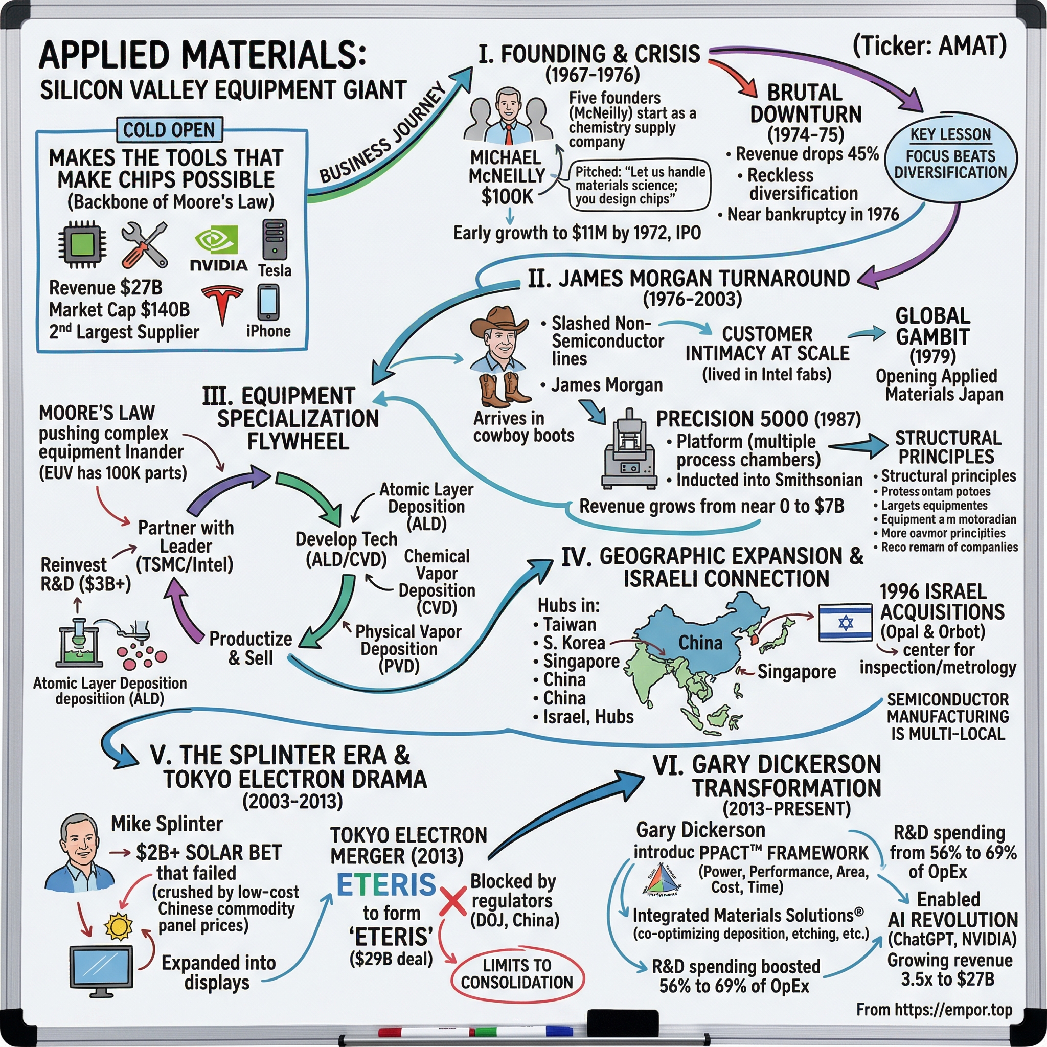
The Cold Open
In November 2023, a quiet building in Silicon Valley received the kind of mail that ends careers and rattles boards. Federal investigators had opened a criminal probe into one of the most important technology companies on Earth — and almost nobody outside the semiconductor industry had heard of it. The allegation was startling in its specificity: that the company had routed hundreds of millions of dollars of advanced chipmaking machinery to China's national champion foundry, 中芯國際 SMIC (Semiconductor Manufacturing International Corporation), through a South Korean intermediary, sidestepping U.S. export controls. The U.S. Attorney's Office for the District of Massachusetts, the SEC, and the Commerce Department all wanted answers.1
This was not a defense contractor or a fly-by-night freight forwarder. It was Applied Materials, a company with a market value north of $140 billion that, by the most reasonable measure, is the single most consequential hardware firm the general public has never heard of. Walk down any street in America and ask passersby to name the company without which there would be no iPhone, no AI data center, no modern automobile — and you would get blank stares, then guesses of Apple, NVIDIA, maybe Intel. Almost no one would say Applied Materials. And yet, in a very real sense, the correct answer is Applied Materials, because the companies people do name all depend on machines that Applied builds.
The Power Paradox
Here is the paradox at the heart of the story. Every advanced microchip on the planet — the silicon inside an iPhone, the controllers running Tesla's Autopilot, and above all the dense racks of 英伟达 NVIDIA H100 and Blackwell processors that power the artificial-intelligence boom — passes through machines that Applied Materials builds. Applied does not design chips and does not manufacture them. It makes the impossibly complex tools that make chips possible, manipulating matter at the scale of individual atoms. If TSMC and Intel are the printing presses of the digital age, Applied is the company that builds the printing presses.
There is an old saying about the California Gold Rush: the people who got reliably rich were not the prospectors panning for gold but the merchants selling them picks, shovels, and Levi's jeans. Applied Materials is the ultimate picks-and-shovels company of the silicon age — except the "shovels" cost tens of millions of dollars each, take years to design, and embody some of the most advanced engineering humanity has ever produced. When the AI gold rush sends chipmakers scrambling to build new fabs, it almost does not matter which chip designer wins. Applied sells the shovels to all of them.
The Investment Thesis Spine
So how do you actually value a business like this? That is the question this episode circles. Applied sits at the absolute throat of global hardware capital expenditure — when the world decides to build chip factories, money flows through Applied. But it is also brutally cyclical, periodically weaponized by governments, and exposed to the slow exhaustion of the physical scaling that drove computing for fifty years. The bull says Applied owns a multi-decade moat in "materials engineering" that only deepens as transistors get harder to build. The skeptic says a chunk of recent demand is a one-time windfall from Chinese customers panic-buying older equipment before the door slams shut. Our job throughout is to keep the analytical posture independent — to hold both ideas at once and ask what the evidence actually supports, rather than reciting either the company's investor-relations gloss or the perma-bear's dismissal.
Episode Map
We will get there in ten movements. First, the near-death founding and the cowboy-boots turnaround that gave Applied its DNA. Second, the structure of the semiconductor-equipment oligopoly — the "Big Five" — and how the economics genuinely work. Third, the M&A engine: the deals that paid off and the blockbusters that regulators killed. Fourth, the Gary Dickerson era and the strategic pivot from making transistors smaller to making them out of new materials. Fifth, the hidden growth vector in advanced packaging and Applied's curious 9% stake in a Dutch company called Besi. And finally, the geopolitical minefield, the bull-and-bear case stress-tested through Porter and Helmer, and the handful of numbers that actually tell you whether the thesis is working. Let's begin where every good turnaround story begins — at the edge of bankruptcy.
II. Turnaround Context: From Chemical Startup to Sunnyvale's "Corpse"
A Company on Life Support
In November 1976, a man named James C. Morgan walked into a company that, by any honest accounting, was already dead. The accounts payable exceeded the receivables. The credit lines were exhausted. The best engineers were updating their résumés. The board had been searching, with grim candor, for what one might call a corpse-recovery specialist — someone willing to take over a failing business and either resurrect it or preside over its funeral. Morgan, a venture investor with a Midwestern engineer's temperament and, depending on who tells the story, a fondness for cowboy boots, took the job.3
It is worth pausing on how unglamorous this moment was. There was no triumphant founding myth here, no garage epiphany, no visionary turning down acquisition offers. Applied Materials in 1976 was a cautionary tale — the kind of company a business-school case study uses to illustrate how not to run a cyclical business. That it became, half a century later, a pillar of the global economy is precisely what makes the turnaround worth dwelling on. The habits a company forms while staring at its own funeral tend to stick.
From Chemistry Startup to Public Company
To understand how Applied Materials got there, you have to rewind nine years. The company was founded on November 10, 1967, by Michael McNeilly and four partners in the orchards of Santa Clara, California, with roughly $100,000 in capital.3 The pitch to the first generation of Silicon Valley pioneers — Fairchild, Intel, Texas Instruments — was elegant and ahead of its time: you focus on designing chips; let us handle the volatile chemistry of materials. Making a semiconductor required depositing and etching exotic films onto silicon wafers, a finicky chemical art. Applied would supply the gases and, increasingly, the machines that controlled those reactions.
It worked, for a while. Applied rode the first semiconductor wave and went public on NASDAQ in 1972, a young company with a few million dollars in revenue and a sense of destiny.3 Then the music stopped. The 1974–75 recession — oil shocks, stagflation, a collapse in electronics demand — hit the chip industry like a sledgehammer. Orders evaporated overnight.
This is the first appearance of a force that recurs in every chapter of Applied's story: the semiconductor cycle. Chipmakers do not spend smoothly. They binge on equipment when demand is hot and capacity is short, then slam the brakes the instant inventories swell, often canceling orders mid-build. An equipment supplier therefore lives on a rollercoaster with no seatbelt — revenue can swing 30% or 40% in a year through no fault of management's. A great equipment company is not one that escapes the cycle; it is one that survives the troughs without doing something stupid. In 1974, Applied did the stupid thing.
And here Applied's management made the classic mistake of a frightened company: instead of cutting to the core, they diversified to chase any revenue they could find. Printed circuit boards. Solar panels. Even medical equipment. Each new venture demanded cash and management attention, and each bled both. The strategic word for this is "diworsification" — the destruction of value that happens when a struggling company convinces itself that more businesses mean more safety, when in fact they mean more places to lose money and fewer dollars for the one thing it does well. By early 1976, the company was, in the brutal phrase that followed it for years, technically solvent but operationally a corpse.
The Morgan Doctrine
Morgan's prescription was radical precisely because it was so simple. He shut down everything that was not semiconductor equipment. Solar, gone. Medical, gone. The diversification that had been sold as prudence was exposed as a death spiral, and he reversed it with a discipline that bordered on the ruthless. Focus over diversification became the law. Then he did something subtler and arguably more important: he pushed Applied's engineers physically inside the customer's factory. Rather than selling a machine and walking away, Applied embedded its people in Intel's fabs to solve the yield problems that kept chipmakers awake at night. The relationship stopped being transactional and became, in a word that recurs throughout this story, intimate.
The third move was the boldest. In the late 1970s, with the company barely off life support, Morgan bet on Japan — establishing Applied's own subsidiary there to serve the rising memory-chip wave, making Applied one of the first U.S. equipment makers to plant a wholly owned flag in the country that was about to dominate DRAM.3 It was the act of a man who had decided that a near-death company should behave like an ambitious one. Consider the contrarianism of it: in the late 1970s, Japanese memory makers were widely feared in America as the competitors who would destroy the U.S. chip industry. Morgan's response was not to retreat behind a wall but to go toward the threat — to sell shovels to the very prospectors everyone else was afraid of. It would take American policymakers another decade to grasp what Morgan understood immediately: that an equipment supplier wins by being indispensable to whoever happens to be winning, regardless of flag.
Morgan would go on to run Applied for the better part of three decades, one of the longest CEO tenures in Silicon Valley history, and would later be awarded the National Medal of Technology. But the relevant point for an investor is not the longevity; it is the template he stamped onto the company in his first eighteen months.
Why does this brief, ancient history matter to an investor in 2026? Because it stamped two traits into Applied's institutional DNA that still explain the business today. The first is radical focus on the equipment business — a hard-won allergy to the diworsification that nearly killed it. The second is physical global presence — putting engineers next to customers wherever in the world they build. Hold those two ideas. They are the keys to understanding how a company that nearly folded in 1976 became the linchpin of the modern chip industry. To see why, we have to leave the history behind and walk onto the floor of a modern semiconductor fab.
III. The Semicap Oligopoly: Core Business, Industry Structure, & The Big Five
Inside the Most Expensive Building on Earth
Step into a leading-edge fab — a building that can cost $20 billion and houses cleanrooms a thousand times cleaner than a hospital operating room. The air is filtered so obsessively that a single speck of dust, invisible to the human eye, can ruin a chip; the engineers wear full-body "bunny suits" not to protect themselves from the chemicals but to protect the wafers from them, from the skin flakes and hair and breath that human beings constantly shed. A bare silicon wafer — a mirror-polished disc about the size of a dinner plate — enters at one end. Over the next two or three months it makes hundreds of trips through a sequence of machines, each performing one exquisitely precise step, before it emerges patterned with tens of billions of transistors, each one far smaller than a virus.
To build a chip is to repeat, over and over, a cycle of deposit a film, pattern it, etch it away, polish it flat, measure everything, repeat. Let's make those abstractions concrete, because the entire investment case rests on understanding who owns which verb. Deposition means laying down an unimaginably thin layer of material — sometimes a film just a few atoms thick — evenly across the whole wafer. Imagine spray-painting a wall so perfectly that the paint is exactly three molecules deep everywhere, with no drips and no thin spots. Lithography means projecting the circuit pattern onto a light-sensitive coating, like an absurdly precise photographic enlarger. Etch means chemically carving away the material you don't want, following the pattern, to leave behind the wires and structures you do — sculpture by subtraction, at the atomic scale. Ion implantation means firing charged atoms into the silicon like a microscopic cannon to change its electrical behavior. Chemical-mechanical planarization, or CMP, means polishing the wafer perfectly flat between layers, because you are building a skyscraper of circuitry and every floor must be level before you pour the next. And metrology and inspection means measuring all of it, constantly, hunting for defects too small to imagine.
Each verb in that sequence is a multi-billion-dollar equipment market. Each is dominated by a handful of companies. And the magic — the reason a chip works at all — is that these hundreds of steps must align with one another to a tolerance of a few atoms. That is the difficulty Applied sells into.
Reading the Segment Mix
Start with what Applied actually sells, because the segment mix tells you where the value lives. In fiscal 2024, Applied reported $27.18 billion in revenue.[^3] The overwhelming majority — roughly three-quarters, about $19.9 billion — came from Semiconductor Systems, the division that builds the tools.[^3] This is the engine of profit, technology, and competitive advantage; everything else is a satellite orbiting it. The second segment, Applied Global Services (AGS), generated north of $5 billion and is the quiet hero of the model: spare parts, maintenance, software, and refurbishment for the installed base of Applied machines running in fabs around the world.[^3] Because it is recurring and high-margin, AGS does something a pure equipment business cannot — it cushions the violent downcycles. The third segment, Display (the tools that make screens for phones and TVs), contributed a little over a billion dollars and is treated, fairly, as a cyclical legacy business.[^3]
The Display segment, by contrast, is the part of the portfolio an investor can largely set aside — and it is instructive why. Making the giant glass panels for televisions and phone screens uses some of the same deposition and etch physics as chipmaking, so it was a natural adjacency for Applied to enter. But display is a brutal, low-margin, boom-and-bust business dominated by a handful of Asian panel makers who themselves struggle for profit, and it lacks the switching-cost dynamics that make the chip business so defensible. Applied keeps it for the engineering synergies and the occasional cyclical upswing, but it is a reminder that even a great franchise can wander into adjacencies that dilute returns — a faint echo of the diversification that nearly sank the company in the 1970s, now kept on a tight leash.
The AGS business deserves a moment more, because investors routinely underrate it. Every Applied machine sold becomes, in effect, an annuity. It needs spare parts, calibration, software updates, and periodic refurbishment for the ten or fifteen years it runs in a customer's fab. Applied has hundreds of thousands of tools installed across the planet, and that installed base throws off service revenue at gross margins far above the equipment itself. The strategic significance is counter-cyclical: when chipmakers slash new-tool orders in a downturn, the existing tools keep running — and keep needing service. AGS is the keel that keeps the ship from capsizing when the equipment cycle turns violent. A growing, sticky service base is, quietly, one of the most important things about the whole company.
The Big Five
Now the part that makes Applied genuinely interesting: it does not compete in a fair fight. The semiconductor-equipment industry is one of the most concentrated oligopolies in modern capitalism — a "Big Five" that, between them, supply nearly every tool in every advanced fab on Earth. They are fierce rivals and, simultaneously, mutually dependent collaborators, because a chipmaker needs all of their machines to work in concert. It is less a battlefield than a cartel of specialists, each guarding its own kingdom while depending on the others to keep the whole system running.
At the top of the pyramid sits ASML, the Dutch firm with an absolute monopoly on extreme-ultraviolet (EUV) lithography — the machines that print the finest patterns. An EUV system is arguably the single most complex machine humans have ever mass-produced; it costs upward of $150 million, ships in dozens of crates, and fires lasers at droplets of molten tin fifty thousand times a second to generate light at a wavelength that almost nothing else in the universe produces on demand. ASML prints the design; no one else on Earth can. This matters for Applied because ASML's monopoly sits at the very leading edge — exactly where Applied's own dominance is most contested.
Then there is Applied itself, the undisputed king of deposition — the art of laying down films of material, atom by atom or molecule by molecule — where it holds commanding share, including roughly 80% of the market for physical vapor deposition. It also holds dominant positions of around 70% in CMP, and a near-monopoly in ion implantation thanks to a deal we will come to shortly. Lam Research is the master of etch, the precise removal of material, and especially the deep vertical channels that make 3D NAND flash memory possible — picture drilling billions of microscopic wells straight down through a stack of more than a hundred layers without the holes wandering off course. 東京エレクトロン Tokyo Electron of Japan dominates the coater/developer "track" tools that work hand-in-glove with lithography, and competes hard in etch, deposition, and the furnaces that bake wafers. And KLA owns process control — the metrology and inspection tools that hunt for defects smaller than a virus and tell the fab whether its other tools are behaving. KLA is the industry's eyes; without it, the other four machines would be operating blind.
Notice the elegant non-aggression in this structure. Applied is the deposition king; Lam is the etch king; the two overlap at the edges but neither has dethroned the other in decades. ASML prints; KLA inspects; Tokyo Electron coats. Each firm's dominance in its core lane is so entrenched that frontal assaults are rare and usually futile. The competition happens at the margins — in adjacent process steps, in new technology inflections where the lanes have not yet been drawn, and increasingly in China, where the rules are different.
The Moat Economics
Here is the question that should occur to any investor: why can't TSMC or Samsung or Intel — companies with engineering talent as deep as anyone's — simply build these tools themselves, or play the suppliers against each other to crush their margins? The answer is the most important idea in the entire business, so let's slow down.
The first reason is switching costs that approach infinity. Qualifying a new tool for production inside a fab is not like swapping a part. It can take a year and millions of dollars, because every machine subtly shapes the atomic characteristics of the wafer. A chipmaker that has spent eighteen months tuning an Applied deposition chamber to hit yield on a 3-nanometer process is not going to rip it out for a competitor's chamber to save a few percent on price — the risk of wrecking the yield on a multi-billion-dollar production line is simply not worth it. Once you are designed into a node, you are designed in for the life of that node. That is pricing power that you do not have to ask for.
The second reason is the sheer scale of the R&D moat. In fiscal 2024, Applied spent about $3.23 billion on research and development — roughly 12% of revenue.[^3] Sit with that number. Applied's annual research budget alone is larger than the entire annual revenue of most second-tier equipment competitors. To catch Applied in deposition, a rival would not just need a clever machine; it would need to replicate decades of accumulated knowledge about how thousands of materials behave under heat, plasma, and pressure — and then keep spending billions a year just to stay level. That is a barrier that money alone cannot quickly buy.
There is a third, subtler reason, and it traces straight back to James Morgan's embedded-engineer doctrine from the 1970s. Applied does not sell tools over a counter; it co-develops them with customers years ahead of production. By the time TSMC or Samsung is ready to ramp a new node, Applied's engineers have spent years inside the joint development program tuning recipes to that specific customer's process. This deep, early entanglement means the relationship is not a vendor relationship at all — it is closer to a co-engineering partnership in which the customer has poured its own scarce R&D time into making Applied's tool work. Walking away does not just incur switching costs; it forfeits a shared investment. The intimacy Morgan pioneered as a survival tactic became, decades later, a structural lock-in.
So what does this mean for an investor? It means Applied's defensibility is structural, not promotional. The concentration is real, the switching costs are observable in customer behavior, and the R&D gap is measurable in dollars. The risk is not that the moat is imaginary — it is that the moat is narrowest at the very leading edge, where ASML's lithography increasingly sets the pace, and that Applied's dominance is strongest in the more commoditizable older nodes. Keep that nuance in your pocket; it becomes the whole ballgame when we get to China. But first, an industry this concentrated has only one obvious way to grow inorganically — by buying up the process steps it doesn't already own.
IV. M&A Capital Deployment & Valuation Benchmarking: The Inorganic Engine
If you cannot easily invent a new process-step monopoly, you buy one. The entire history of semiconductor-equipment consolidation is the story of giants acquiring smaller specialists to add another lane to the toll road. Applied has run this playbook for decades, and its record is genuinely instructive — a mix of disciplined opportunism and at least one deal that Wall Street swore was a blunder. The discipline of testing an acquirer's record is straightforward: did they buy scarce assets or commodity ones, did they pay for monopoly or for revenue, and did the cash flows ultimately vindicate the price? Run Applied through that filter and a clear pattern emerges.
Semitool: Buying When Others Are Paralyzed
Consider the timing of the Semitool acquisition in 2009. Applied bought the company — a specialist in electrochemical deposition, the technique used to plate the copper wiring that connects transistors — in the depths of the global financial crisis, when asset prices were on the floor and most of the industry was hoarding cash.3 Buying a strategic technology cheaply, in cash, precisely when everyone else is paralyzed by fear is the textbook definition of disciplined capital allocation. The deal was small, but it was a tell: Applied's management understood that the best time to buy is when the cycle has scared everyone else away.
Varian: The "Overpriced" Deal That Wasn't
The defining acquisition, though, was Varian Semiconductor in 2011, a roughly $4.9 billion all-cash deal that remains the largest Applied has ever completed.4 And at the time, the reaction was not applause — it was alarm. Applied paid a premium of more than 50% over Varian's pre-deal price, a multiple that, by the standards of the day's comparable transactions, looked rich — somewhere around four-and-a-half times Varian's trailing revenue and roughly eighteen times its earnings before interest, taxes, depreciation and amortization, at a moment when comparable equipment deals were changing hands closer to twelve to fifteen times. The Street's verdict was blunt: Applied had overpaid.
Here is where independent analysis has to override the original headlines. What Applied actually bought was a near-monopoly in ion implantation — that step where dopant atoms are fired into silicon, a process with no real alternative and brutally high barriers to entry. Then Applied did the thing it does best: it ran Varian's technology through its own global sales-and-service machine, the AGS engine. A near-monopoly product distributed through a worldwide service network is a cash-generation flywheel, and over the following decade Varian's tools threw off billions in high-margin revenue. The lesson is not that premiums are good — it is that price and value are different questions. Applied paid a high price for a genuinely scarce asset and let compounding cash flow vindicate the decision. An acquirer that overpays for a commodity destroys value; an acquirer that overpays for a monopoly often looks brilliant in hindsight. The discipline is in telling the two apart.
Besi: The 9% Stake as a New Kind of Move
The most recent and most revealing move came in April 2025, and it was not an acquisition at all. Applied announced it had purchased a 9% stake in BE Semiconductor Industries — Besi, a Dutch maker of chip-assembly equipment — as a strategic investment rather than a buyout.5 Why take a minority position instead of swallowing the company whole? Two reasons, and both matter. The first is strategic: the technology the two firms are co-developing, called hybrid bonding, requires marrying Applied's front-end expertise in ultra-clean wafer surfaces with Besi's back-end mastery of placing tiny chips with sub-micron accuracy. A 9% stake plus a deepened partnership locks in that collaboration without the integration risk and regulatory peril of a full merger. The second reason is the one that haunts this entire chapter: Applied has learned, painfully, that the era of giant equipment mergers is over. To understand why a 9% stake is now the sophisticated move, we have to look at the two blockbuster deals that regulators blew up.
V. The Failed Blockbuster Mergers & The Regulatory Wall
The Eteris Dream
In September 2013, Applied Materials and Tokyo Electron stood on a stage and announced something audacious: a merger of equals worth roughly $29 billion that would create an entirely new company. They even had a name for it — Eteris, a coinage meant to evoke "eternal" and "innovation."6 On paper it was breathtaking. Combine Applied's dominance in deposition with Tokyo Electron's strength in etch, clean, and track tools, and you would create a colossus controlling well over a quarter of the entire global equipment market — a company that touched nearly every step of making a chip outside of lithography.
The two companies were not casual about it. They spent nineteen months and, by reasonable estimates, hundreds of millions of dollars planning the integration — knitting together org charts, product roadmaps, and supply chains across two continents and two corporate cultures. And then, in April 2015, they walked away. The merger was terminated, and the press release blamed concerns from the U.S. Department of Justice.7
The deeper truth is that regulators on multiple continents had decided the combined entity would simply hold too much power over the world's chipmakers. The U.S. Department of Justice signaled it would not clear the deal on acceptable terms, and China's antitrust authority was understood to be equally hostile. The fear was straightforward: a single company controlling more than a quarter of the equipment a chipmaker needs would have too much leverage to raise prices on customers who had nowhere else to turn. The very switching costs and concentration that make Applied such a wonderful business are also what made the merger un-clearable. The moat, in a sense, was too good to be allowed to get bigger.
The lesson was unmistakable and, for Applied, expensive: the antitrust authorities now view the equipment industry as so concentrated that horizontal mergers between its largest players are effectively forbidden. You cannot combine two of the Big Five. The strategic ceiling was now visible, and it was lower than anyone at Applied had assumed.
The Kokusai Death by a Thousand Cuts
If Eteris was the dream that died of antitrust, the Kokusai Electric saga was death by a thousand bureaucratic cuts. In 2019, Applied agreed to buy Kokusai — a Japanese leader in the batch-processing furnaces used to deposit films on many wafers at once — from the private-equity firm KKR, in a deal that grew to around $3.5 billion.8 This was not a merger of titans; it was a sensible bolt-on. But it required approval from China's antitrust regulator, 国家市场监督管理总局 SAMR, and that approval never came. Month after month, the clock ran. By March 2021, with the deadline expired and Chinese clearance still nowhere in sight, Applied was forced to terminate the deal and pay KKR a $154 million breakup fee for the privilege of having tried.8
The Strategic Lesson
Read those two episodes together and a strategy comes into focus — or rather, the absence of one particular strategy. The path of horizontal megadeals is closed. The regulators in Washington and Beijing have built a wall, and that wall now shapes everything about how Applied deploys capital. It is precisely why the company's modern playbook looks the way it does: minority stakes like the Besi investment, organic capacity expansion such as the EPIC Center for collaborative R&D that Applied unveiled in 2023,9 and, above all, aggressive return of cash to shareholders — Applied repurchased $3.82 billion of its own stock in fiscal 2024 alone.[^3] When you cannot buy your competitors, you buy your own shares and you build your own labs. Whether that is the disciplined response of a mature franchise or a sign that the easy growth is behind it is a fair debate — but the constraint is real, and it was imposed from outside. The man who has had to navigate that constraint, and who reoriented the entire company while doing so, took the top job in 2013.
VI. The Gary Dickerson Era: Materials-Led Scaling & The PPACt Framework
When Gary Dickerson became CEO of Applied Materials in September 2013, he inherited a company in the middle of the doomed Tokyo Electron merger and an industry quietly approaching a wall. Resist the temptation to write the hagiography; Dickerson is best understood not through his personality but through his incentives, his record, and one genuinely consequential strategic bet.
A word on the man's path, because it is unusual. Dickerson did not arrive through finance or marketing; he came up through operations and manufacturing, with a stint running the disk-drive and chip-equipment maker Varian — yes, the same Varian Applied had acquired — and before that the lithography company Applied later folded in. He is, by reputation, an operator's operator: relentless on yield, fluent in the physics, more comfortable on a fab floor than a stage. That background matters because the bet he was about to make was not a financial-engineering bet or a branding exercise. It was a bet about the physics of how chips would be built for the next twenty years, and it required a CEO who actually understood the chemistry.
An Owner-Operator's Incentives
Start with the incentives, because they are unusually clean. As of mid-2026, Dickerson directly held 1,678,164 shares of Applied Materials, a stake worth well over a billion dollars at prevailing prices — a holding large enough that his personal wealth rises and falls with the same stock the rest of the shareholders own.10 His pay reinforces the alignment. In fiscal 2025 his reported total compensation was roughly $29.65 million, but the structure matters more than the headline: the overwhelming majority is variable and performance-based, and the large bulk of it is delivered in long-term equity rather than cash.10 Crucially, the performance share units that make up most of his potential payout vest only against two hard, externally verifiable metrics — Applied's non-GAAP operating margin and its total shareholder return measured relative to the S&P 500 information-technology index.10 In plain English: Dickerson does not get paid for a rising tide that lifts all chip stocks; he gets paid for beating his peers and for running the business efficiently. That is the kind of structure an activist would design, and it is already in place.
There is a fair skeptical question to ask about any CEO who has held the job for more than a decade: is the alignment real, or is it a long-tenured executive extracting rents while the board waves it through? Two facts push back. First, the relative-TSR metric means a generic semiconductor rally does not pay Dickerson — he has to beat the tech index, which is a high bar in a sector that has minted many winners. Second, the sheer size of his retained equity stake means selling out and coasting was always an option he declined; he has kept the overwhelming majority of his wealth riding on the same shares as outside holders. None of this proves he is worth $29.65 million in a given year — reasonable people can argue executive pay is inflated industry-wide — but the structure is about as well-aligned as large-cap CEO pay gets.
The Wheezing of Moore's Law
Now the strategy. When Dickerson took over, the engine that had powered the chip industry for half a century — making transistors physically smaller, year after year, mostly by improving lithography — was sputtering. Transistors had shrunk to the point where electrons leaked across barriers and heat became unmanageable. The most visible symptom was Intel's catastrophic, multi-year struggle to move from its 14-nanometer to its 10-nanometer process, a delay that became the canary in the coal mine for the entire idea of effortless miniaturization. Moore's Law, the metronome of progress, was wheezing.
To grasp why this was an opportunity rather than a threat for Applied, you have to understand the division of labor inside a chip's history. For decades, the hero of miniaturization was lithography — better lenses and shorter wavelengths of light let you print ever-finer lines, and everything else followed. In that world, the lithography company (eventually ASML) captured the glory and a rising share of the value. But when lithography hit physical limits, the industry could not simply stop improving. It had to find performance gains elsewhere — and "elsewhere" meant new materials and new three-dimensional shapes. That shift moved the locus of innovation away from pure pattern-printing and toward exactly the things Applied does.
Dickerson's insight — and it is a genuine reframing, whatever you think of the marketing around it — was that if you can no longer make transistors meaningfully smaller, you must make them better by building them out of new materials and new three-dimensional structures. Lithography prints the pattern, but it is materials engineering that determines what the transistor is actually made of and how it is shaped. And materials engineering — deposition, etch, modification, polishing — is exactly Applied's home turf. The industry's pain became Applied's opportunity.
The clearest example is the transistor's own evolution. For years transistors were essentially flat. Then the industry went vertical with "FinFET" designs, standing the transistor up like a fin to control the current better. The next leap, "gate-all-around," wraps the controlling gate entirely around a stack of nanometer-thin sheets — and building those structures requires depositing and selectively removing alternating layers of different materials with atomic precision, then adding "backside power delivery" that routes electricity from underneath the wafer. Every one of those innovations is a deposition-and-etch problem, not a lithography problem. Each new architecture, in other words, increases the dollar value of the materials-engineering tools required to build a chip — which is to say, it increases Applied's addressable content per wafer. That is the mechanism beneath the slogan.
The PPACt Framework
Applied wrapped this in a framework it calls PPACt: Power, Performance, Area, Cost, and time-to-market. The "t" is the tell — Applied's argument is that the old game of optimizing for area (smaller is better) has given way to a multi-dimensional game where new materials can improve power and performance even when the transistor stops shrinking. The commercial expression of this idea is what Applied calls Integrated Materials Solutions — combining several process steps, such as deposition, etch, cleaning, and measurement, inside a single connected vacuum system so the wafer never sees contaminating air between steps. The pitch to customers is that as transistors grow more delicate, integration and cleanliness become worth a premium, and only a company that owns many of the steps can deliver it.
Does the Strategy Show Up in the Numbers?
Does the strategy show up in results? Under Dickerson, Applied's revenue grew from about $7.5 billion in fiscal 2013 to $27.18 billion in fiscal 2024, while operating margins roughly doubled into the high-20s percent range.[^3] That is not a rerating driven by hype; it is a tripling of the business with expanding profitability across more than a decade — the signature of real operating leverage and pricing power, not just a friendly cycle. The honest caveat is that some of that growth coincided with an unprecedented global capex boom, and a skeptic would want to separate Dickerson's strategy from the rising tide. But the margin expansion is harder to dismiss: it suggests Applied is capturing more value per dollar of customer spending than it used to, which is what you would expect if the materials-led narrative were genuinely translating into stickier, higher-content tools. And nowhere is that content growing faster than in a corner of the industry that used to be an afterthought.
VII. Advanced Packaging & Hybrid Bonding: The "Hidden" Growth Engine
For decades, "packaging" was the unglamorous final step of chipmaking — the part where a finished silicon die got encased in plastic and given metal legs, work so routine it was often shipped off to low-cost subcontractors in Asia. It was the loading dock of the semiconductor factory, the place where the real work was already done. Then the AI boom broke the rules of physics, and packaging became one of the most strategically important — and fastest-growing — battlegrounds in the entire industry. On Applied's own earnings calls, management now lists advanced packaging alongside gate-all-around transistors and backside power delivery as one of the major "technology inflections" expanding its addressable market — a striking promotion for what used to be an afterthought.13
The Reticle Wall
The reason is a hard limit called the reticle. A lithography machine can only print a pattern up to a certain maximum size in a single shot — roughly the size of a large postage stamp. For most of history that was plenty. But modern AI accelerators, like NVIDIA's Blackwell processors, are so enormous and so transistor-hungry that they bump up against this reticle limit. You physically cannot print the whole thing as one monolithic chip. So the industry pivoted to a different idea: build several smaller chips — "chiplets" — and stitch them together into one super-chip. A logic die here, stacks of high-bandwidth memory there, perhaps an optical connector, all assembled onto a dense silicon base called an interposer. The jargon for this is heterogeneous integration; the plain-English version is that if you can't carve a statue from one block of marble, you assemble it from precisely fitted pieces.
Hybrid Bonding: Welding Chips at the Atomic Level
How you connect those pieces is where the money and the moat are. The traditional method uses micro-bumps — tiny balls of solder between the chips. But bumps take up space, limit how densely you can pack the connections, and waste power. The next generation eliminates them entirely. Hybrid bonding fuses copper pad directly to copper pad, welding two chips together at near-atomic flatness so that current flows as if through a single piece of metal. It allows vastly denser connections and lower power — and for the most demanding AI and memory chips, it is increasingly the only way to get the performance designers need. The market for it has been growing at something like a 40% compound rate, off a small base, which is exactly the profile of a technology crossing from novelty into necessity.
To make the stakes vivid: hybrid bonding requires the two surfaces to be so flat and so clean that, when pressed together and gently heated, the copper atoms on each side migrate across the boundary and effectively become one piece of metal — a cold weld at the atomic scale. A single particle of contamination, or a surface that deviates from flatness by a few nanometers, ruins the bond. This is why it sits at the intersection of two disciplines that historically never met.
Why Besi, and Why a Stake
This is where the Besi relationship pays off. Hybrid bonding sits awkwardly between two worlds: it needs the spotless, atomically controlled wafer surfaces that are Applied's front-end specialty, and the sub-micron mechanical precision of placing one die onto another that is Besi's back-end specialty. Neither company could easily build the whole solution alone. So they have been collaborating since 2020 to co-develop integrated hybrid-bonding equipment, and in 2025 they unveiled the fruit of it — a system Applied calls Kinex, billed as the industry's first fully integrated die-to-wafer hybrid bonding tool, combining surface preparation, bonding, and metrology in a single machine.115 Applied supplies the clean front-end surface preparation and the barrier films; Besi supplies the placement accuracy. The 9% equity stake taken in April 2025 is the financial expression of a co-optimization that is hard for a pure-play packaging competitor to replicate.5
It is worth being clear-eyed about the competitive field, because advanced packaging is not an Applied monopoly the way deposition is. The chipmakers themselves, above all TSMC with its proprietary "CoWoS" packaging platform, have built deep in-house capability and guard it jealously, since for the AI era packaging has become a source of competitive differentiation rather than a commodity to outsource. Other equipment players, including the assembly-tool specialists and Applied's own rivals, are racing into hybrid bonding as well. Applied's bet is that integrating front-end process control with back-end placement gives it a structural edge — but that thesis is, at this stage, partly a promise. The falsifying evidence to watch for would be the major foundries standardizing on hybrid-bonding tools from someone other than the Applied-Besi partnership, or keeping the most valuable steps inside their own four walls. Until production volumes scale, the moat in packaging is a hypothesis with encouraging early data, not a settled fact.
What should an investor take from this? Advanced packaging is the clearest example of Applied's central claim actually coming true: as the easy transistor shrink slows, more of the value in a chip migrates toward materials engineering and assembly — Applied's territory. It is a credible, evidence-backed growth vector rather than a slogan. The honest counterpoint is that it is still a relatively small slice of revenue today, and the Besi structure means Applied shares the economics rather than owning them outright. It is optionality with real substance, not yet a second engine. Which brings us to the part of the story where substance collides with geopolitics.
VIII. The Geopolitical Minefield & The China Dilemma
A Dangerous Concentration
For a stretch of 2024, the single largest source of Applied Materials' revenue was not the United States, not Taiwan, not Korea — it was China. At its peak, China accounted for roughly 43% of the company's total sales in a quarter, up from around 21% a year earlier.12 For a company sitting at the center of a U.S.-China technology war, that is a staggering and uncomfortable concentration. Understanding why it happened — and why it is already reversing — is essential to understanding the risk.
The surge had a specific cause. As Washington tightened export controls to choke off China's access to the most advanced chipmaking tools, Chinese manufacturers responded by buying everything they were still allowed to buy, as fast as they could. They could not get cutting-edge 3-nanometer equipment, so they poured capital into the mature "legacy" nodes — 28 nanometers and older — that power cars, appliances, industrial sensors, and the broad mass of everyday electronics. The goal was self-sufficiency in the chips China could realistically make domestically, and the result was a historic buying spree for exactly the kind of older deposition, etch, and implant tools that Applied sells in volume. A wall meant to slow China down created, in the near term, a flood of orders.
There is a deep irony worth naming here. Export controls designed to contain China's chip industry produced, as a near-term side effect, a windfall for the American companies they were meant to enlist. By forbidding the sale of cutting-edge tools while leaving the older ones legal, Washington effectively herded Chinese demand into exactly the mature-node equipment that firms like Applied sell in bulk. Policy intended to slow China down briefly inflated the revenue of the company now at the center of an export-control scandal. Which brings us to the scandal itself.
When the Wall Caught Applied
Then the wall caught Applied itself. The criminal probe that opened our story was not an abstraction, and in February 2026 it produced a concrete and painful resolution. Applied agreed to pay a civil penalty of about $252.5 million to the U.S. Commerce Department's Bureau of Industry and Security to settle charges that it had violated export controls — the second-largest such penalty the agency has ever imposed, behind only a $300 million fine levied on Seagate in 2023.2 The conduct at issue: shipping ion implanters and related equipment, on 56 occasions across 2021 and 2022 and worth roughly $126 million, from a plant in the United States to a subsidiary in South Korea, from where they were forwarded to SMIC after that company had been placed on the U.S. Entity List.2 As part of the settlement Applied agreed to outside audits of its compliance program and confirmed it had terminated the employees responsible.2 The $252.5 million was a financial slap, not a body blow, to a company this size — but it is a permanent stain on the compliance record, and it crystallizes a structural truth: a business this exposed to China is a business one regulatory decision away from a bad quarter or a worse headline.
The Skeptic's Stress Test
Now run the skeptic's stress test, because it is the right one. The bear case has two prongs. The first is the China pull-forward argument: that the 40%-plus revenue share was never sustainable, that it represented demand pulled forward from future years by panic and subsidy, and that when China finishes building out its legacy capacity, those orders will collapse and leave Applied facing an ugly cyclical air pocket. This is not hypothetical — on Applied's own second-quarter fiscal 2025 earnings call, management told investors it expected lower spending in China for the year, with both DRAM and mature-logic investment down, even as leading-edge demand elsewhere grew.13 In other words, the reversal the bears predicted has begun, and the company is acknowledging it in plain language. The question is whether AI-driven leading-edge demand grows fast enough to fill the hole that China leaves.
The second prong is the indigenous threat. China's domestic equipment champions — 北方华创 NAURA in deposition, etch, and clean, and 中微公司 AMEC in etch and CVD — are climbing the technology ladder with state backing and aggressive, subsidized pricing. They cannot yet touch Applied at the leading edge. But in China's vast legacy-node market, they are increasingly good enough, and "good enough plus heavily subsidized plus politically favored at home" is precisely the combination that erodes a foreign incumbent's share over time.
This is the textbook pattern of how incumbents lose, and it deserves to be taken seriously rather than waved away. Clayton Christensen's framework for disruption describes exactly this: a cheaper, initially inferior competitor establishes itself at the low end of a market, where the incumbent is least motivated to fight, and then marches upmarket as its technology matures. NAURA and AMEC are following that script with the added rocket fuel of a national government determined, as a matter of strategic survival, to make China self-sufficient in semiconductors — a goal explicitly elevated under Beijing's industrial policy. Applied's own management has acknowledged on its calls that it underperformed the overall China market in 2024 because of the access restrictions on U.S. firms, which is a polite way of saying that local competitors took share Applied was forbidden to defend.13 The leading edge may be safe for years. The legacy base is contested today. The very demand boom that inflated Applied's China revenue is also funding the competitors most likely to take that revenue away. For an investor, this is the crux: Applied's China business is simultaneously its biggest recent tailwind and its most concentrated long-term vulnerability, and the two cannot be separated. So how should a disciplined investor frame the whole picture?
IX. Playbook & Strategic Powers: 5 Forces, 7 Powers, & Investor KPIs
Helmer's 7 Powers
Strip away the narrative and look at Applied Materials through the cold lens of competitive-strategy frameworks, and the picture sharpens considerably. Hamilton Helmer's 7 Powers is a useful scalpel here, because it forces you to name which advantage you are actually relying on.
The clearest power is scale economies, expressed through R&D. Applied's multi-billion-dollar annual research budget functions as a moat by sheer magnitude — a smaller rival simply cannot fund enough materials experiments to close the gap, and the gap compounds. The second, and arguably the deepest, is switching costs: the year-long, multi-million-dollar qualification process that locks a customer into Applied's tools for the life of a process node, with yield risk so severe that swapping suppliers mid-node is close to unthinkable. The third is a cornered resource — not a patent or a mine, but a "materials library" of decades of proprietary recipes: how thousands of films behave under specific conditions of plasma, heat, and pressure. That accumulated, hard-won know-how cannot be bought or quickly reverse-engineered. A fourth, more contestable power is counter-positioning in advanced packaging: Applied's integrated front-end-to-back-end hybrid-bonding approach is structurally awkward for a pure-play packaging competitor to copy without an Applied-like front-end franchise. The honest assessment is that the first three powers are strong and observable; the fourth is real but still emerging.
Porter's Five Forces
Porter's Five Forces tells a complementary story with one delicious paradox. The bargaining power of buyers looks enormous — Applied's customers are extraordinarily concentrated, with a handful of names like TSMC, Samsung, and Intel making up a large share of revenue, and in principle a concentrated customer base can squeeze a supplier hard. Yet in practice those buyers have nowhere else to go for critical deposition, CMP, and implant steps, so their theoretical power rarely converts into actual margin pressure. The threat of new entrants, meanwhile, is essentially zero — the combination of capital intensity, patent thickets, and the materials library is insurmountable for a startup. The genuine competitive tension comes not from new entrants or buyers but from the adjacent rivals — Lam, Tokyo Electron, KLA — each strong in its own lane, and from the state-funded Chinese challengers nibbling at the bottom. This is an industry where the front door is bolted shut but the windows are worth watching.
Myth vs Reality
Three consensus narratives deserve to be fact-checked against the evidence, because each is half-true in a way that misleads.
Myth one: "Applied is an AI stock." The reality is more textured. Applied benefits enormously from AI, but the benefit is indirect and diffused across the whole capex cycle — it sells the tools that build the chips that run AI, not AI itself. In the near term, a meaningful slice of recent revenue came not from leading-edge AI logic but from Chinese mature-node buying that has little to do with artificial intelligence. The leading-edge AI tailwind is real and growing, as management has emphasized on recent calls, but an investor who treats Applied as a pure-play AI bet is conflating a structural, slow-moving capex franchise with a fast-moving end-market it merely supplies.13
Myth two: "Moore's Law is dead, so Applied is in trouble." This inverts the truth. The slowdown in classic lithographic shrinking is precisely what shifted value toward materials engineering — new transistor architectures, new materials, and advanced packaging — which is Applied's home ground. The death of easy shrinking is a tailwind for Applied's content-per-wafer, not a headwind, even as it pressures the chipmakers themselves. The risk to Applied is not that Moore's Law slows; it is the opposite scenario, in which some breakthrough makes chips dramatically cheaper to build with fewer process steps.
Myth three: "The China penalty settles the risk." The $252.5 million payment closes one chapter, but the underlying exposure — roughly two-fifths of revenue at the peak, concentrated in a geopolitically contested market, with subsidized local competitors rising — is structural and ongoing. The fine is a sunk cost; the concentration is a live one.
The Activist's Line of Attack
So what would an activist or short-seller actually attack? Three things, integrated rather than itemized. First, the China concentration and the compliance failure it exposed — a governance and disclosure question as much as a demand question, now with a $252.5 million penalty to point at. Second, the capital-allocation pivot to buybacks: with megadeals foreclosed by regulators, Applied is returning enormous cash to shareholders, and a skeptic would ask whether that reflects genuine discipline or a quiet admission that the company has run out of high-return places to deploy capital internally. Third, the cyclicality itself — the risk that record recent results flatter a business that is closer to a peak than a trough. None of these are fatal, but a thoughtful long should be able to answer all three.
The Three KPIs That Matter
That leaves the practical question: if you can track only a few numbers, which ones actually tell you whether the thesis is intact? Three stand out. The first is non-GAAP operating margin — the cleanest single read on pricing power and operating leverage; sustained margins in the high-20s to mid-30s percent range signal that the materials-engineering moat is holding, while erosion would be the first sign that Chinese competition or mix is biting. The second is AGS revenue growth and its attach rate — because the service business is high-margin and recurring, a steadily growing installed-base service stream is the shock absorber that determines how brutal the next downcycle feels. The subtlety worth watching is the mix within AGS: Applied has been steadily converting one-off, transactional service into long-term subscription agreements that renew automatically, which makes the revenue both stickier and more visible. A rising share of subscription-based service contracts, and a rising attach rate on newly shipped tools, would be strong evidence that the installed base is compounding into a genuine annuity rather than a collection of one-time repairs. If AGS growth stalls while the equipment cycle is also turning down, that is the configuration that should worry a long-term holder most, because it would mean the keel is no longer steadying the ship. The third is the share of revenue coming from China — the single best gauge of geopolitical risk. A gradual decline from the 40s back toward a sustainable 20-something percent, without a collapse in total revenue, would be the bullish signal that demand is healthily rebalancing toward U.S., European, and Korean reshoring. A disorderly drop, with total revenue falling alongside it, would confirm the bears. Watch those three, and you will know more than most.
X. Conclusion & Epilogue
Return, finally, to the spine of the whole story. Applied Materials is not merely a participant in the AI and silicon boom — it is one of its physical gatekeepers, the company whose machines stand between a slice of sand and a thinking computer. That position is rare, structurally defended, and, on the evidence of expanding margins through a decade of transformation, genuinely valuable rather than merely asserted.
But this episode has tried to hold the bull and the bear in the same hand. The materials-engineering moat is real and arguably deepening as transistor scaling slows and value migrates toward deposition, new materials, and advanced packaging — Applied's home ground. At the same time, the company is more exposed than almost any peer to a single geopolitical fault line, it has just paid one of the largest export-control penalties in U.S. history, and a meaningful slice of its recent demand is already reversing as China's buying spree cools and China's own equipment champions climb the ladder Applied helped build. Both things are true at once. The interesting companies usually are.
It is worth naming the risk radar plainly, because an equipment company carries a distinctive risk profile. The dominant risk is not technological disruption — Applied's moat is genuinely deep — but cyclicality colliding with concentration. A simultaneous downturn in chip demand and a structural decline in Chinese orders could compress revenue sharply in a single year, and because so much of Applied's cost base is fixed R&D and skilled engineering it cannot easily flex, margins would feel it. Layered on top are the live geopolitical risk (further export rules could cut either way), the execution risk of betting on still-young inflections like hybrid bonding, and the governance overhang exposed by the export-control case. None of these is the kind of existential threat that kills a franchise; together they are the kind of turbulence that makes the stock a rollercoaster even when the long-run trajectory is up. The cushion against all of it is the recurring services base — which is exactly why it sits among the handful of numbers worth watching.
So why would Applied win from here, stated as a testable claim rather than a hope? The strongest version of the bull case is mechanical, not rhetorical: each new transistor architecture and each step toward heterogeneous, packaged designs increases the dollar value of materials-engineering tools required per wafer, and Applied owns the largest share of those tools, defended by switching costs visible in customer behavior and an R&D budget larger than rivals' entire revenue. If that mechanism holds, Applied's content grows even in a world where the number of wafers grows only modestly — the company captures more of each chip's manufacturing cost over time. The bear case does not dispute the moat; it disputes the price and the cycle — that today's results sit near a China-inflated peak, that a downturn could be severe, and that subsidized local competition will slowly hollow out the legacy base. The evidence currently supports the moat thesis on the leading edge and the concentration risk on the trailing edge simultaneously, which is why the honest conclusion is a tension rather than a verdict.
The enduring lesson sits at a higher altitude than any quarter's results. In an age intoxicated by software, platforms, and digital abstraction, it is worth remembering that all of it ultimately runs on physical reality — on the ability to move single atoms onto a slice of silicon with a precision that borders on the miraculous. Applied Materials is one of the few organizations on Earth that has mastered that act. Whether mastery of the physical world translates into durable returns from here depends on the numbers we just named — the margins, the services base, and that stubborn, telling China line. The atoms, at least, are not going anywhere.
References
-
Applied Materials under U.S. criminal probe for shipping to China — Reuters, 2023-11-16 ↩
-
Applied Materials to pay $252.5M to settle export violations — Manufacturing Dive, 2026-02-12 ↩↩↩
-
Applied Materials Completes Acquisition of Varian Semiconductor Equipment Associates — Applied Materials, 2011-11-10 ↩
-
Applied Materials Announces a Strategic Investment in BE Semiconductor Industries — Applied Materials, 2025-04-14 ↩↩↩
-
Applied Materials and Tokyo Electron Announce Agreement to Merge — Applied Materials, 2013-09-24 ↩
-
Applied Materials and Tokyo Electron Agree to Terminate Merger Agreement — Applied Materials, 2015-04-27 ↩
-
Applied Materials Announces Termination of Kokusai Electric Acquisition Agreement — Applied Materials, 2021-03-29 ↩↩
-
Applied Materials Announces EPIC Center to Accelerate Semiconductor Manufacturing Innovation — Applied Materials, 2023-05-22 ↩
-
Applied Materials Inc — Form DEF 14A Proxy Statement, FY2025 — SEC, 2025-01 ↩↩↩
-
Applied Materials and Besi to Co-Develop Integrated Hybrid Bonding Equipment Solutions — Applied Materials, 2020-10-21 ↩
-
Applied Materials under U.S. criminal probe for shipments to China's SMIC — CNBC, 2023-11-16 ↩
-
Applied Materials Second Quarter Fiscal 2025 Earnings Press Release (Form 8-K) — SEC, 2025-05-15 ↩↩↩↩
 RSS Feed
 Spotify
 Apple Podcasts
 Amazon Music
 Audible
 YouTube