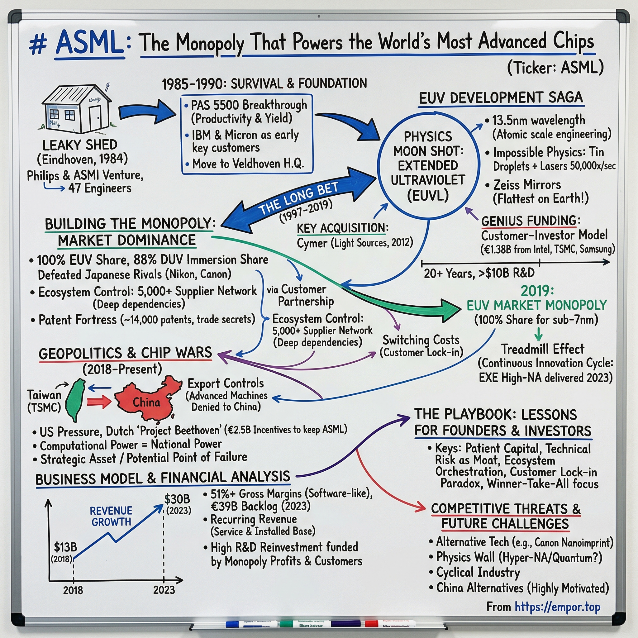
ASML: The Monopoly That Powers the World's Most Advanced Chips
I. Introduction & Opening
Picture this: A single Dutch company holds absolute power over humanity's technological future. Not through military might or political influence, but through machines so complex that only 140 of them exist on Earth. These $200-300 million behemoths, weighing 180 tons and requiring three Boeing 747s to transport, are the sole gateway to manufacturing the chips that power artificial intelligence, smartphones, and virtually every piece of advanced technology we touch.
ASML is the sole supplier in the world of extreme ultraviolet lithography (EUVL) photolithography machines that are required to manufacture the most advanced chips. ASML completely dominates the EUV lithography market, with a 100% market share. No other company currently produces EUV lithography machines, making ASML the only supplier for the world's most advanced chipmakers. This isn't market leadership—it's complete and utter monopolization of the most critical technology in the semiconductor supply chain.
The numbers tell a story of dominance rarely seen in modern capitalism. ASML dominates the semiconductor lithography market with a 100% share in EUV and an 88% share in DUV Immersion. ASML's EUV machines have experienced a significant surge in demand in recent years, driven by modern electronics' increasing complexity and performance requirements. This has translated into steady revenue growth for the company, reaching $30 billion in 2023, up from $13 billion five years earlier. As of November 2024, ASML was the fourth most valuable company in Europe, and the second most valued European tech company, with a market capitalization of about US$264 billion.
But ASML's journey to monopoly status wasn't predestined. It began in the least auspicious way imaginable: In 1984, electronics giant Philips and chip-machine manufacturer Advanced Semiconductor Materials International (ASMI) created a new company to develop lithography systems for the growing semiconductor market. Called ASM Lithography, we began our days inauspiciously, located in a leaky shed next to a Philips office in Eindhoven, the Netherlands. Yes, you read that correctly—the company that would eventually determine whether Intel, TSMC, or Samsung could produce next-generation chips started in a literal leaky shed.
How does a ragtag team of 47 engineers from a struggling Dutch conglomerate evolve into the undisputed kingmaker of the semiconductor industry? How did they bet $10 billion and 20 years on a technology that many thought impossible? And why, despite their monopoly power and eye-watering margins, has no competitor emerged to challenge them?
This is the story of the most important company you've probably never heard of—until the chip wars made them famous. It's a tale of patient capital, impossible physics, and the peculiar dynamics that create natural monopolies in the deepest layers of the technology stack. Welcome to the world of ASML, where light itself is engineered at the atomic level, and where the future of computing depends on mirrors so flat that if they were scaled to the size of Germany, their highest point would be less than a centimeter tall.
II. Origins: The Philips Era & Pre-History (1970s–1984)
The rain hammered against the windows of Natlab, Philips' legendary research facility in Eindhoven, as a small team of engineers huddled around a prototype that refused to work. It was 1978, and they were trying to solve a problem that would determine whether Europe would have any role in the coming semiconductor revolution. The Silicon Repeater, as they called it, was supposed to revolutionize chip manufacturing. Instead, it sat there, stubbornly inert, while American and Japanese competitors raced ahead.
Founded by father and son Gerard and Frederik Philips in 1891, by the 1970s it had interests in lighting, in audiovisual products and in healthcare systems. Philips wasn't just another electronics company—it was a sprawling industrial empire, a European answer to General Electric. But by the 1970s, cracks were showing in the empire's foundation. The company that had pioneered everything from light bulbs to compact cassettes was struggling to find its place in the semiconductor age.
The conglomerate's semiconductor ambitions weren't merely opportunistic. In 1975, the company acquired Signetics, founded by employees of Fairchild Semiconductor in 1961. The acquisition of Signetics made Philips the second-largest manufacturer of semiconductors in the world. Think about that for a moment—Philips was once the world's second-largest chip manufacturer. Today, it doesn't even make chips. This transformation from semiconductor giant to healthcare company is one of the great untold stories of industrial evolution.
At the heart of Philips' semiconductor strategy was Natlab (short for Natuurkundig Laboratorium), their physics laboratory that had become legendary for innovation. The story of ASML is largely one of its technology, and that technology starts in Natlab with the development of the first Silicon Repeater. The Silicon Repeater was a machine that would move a silicon wafer so that an image could be repeatedly projected onto it by an optical mechanism held above the wafer. To make sense of the Silicon Repeater, though, we have to understand how integrated circuits were being made before it arrived.
The problem Philips faced was endemic to large conglomerates: brilliant technology trapped in bureaucratic amber. They had developed sophisticated lithography systems—the PAS 2000 series—that could theoretically compete with anything from Japan or America. But theoretical excellence doesn't pay bills. The machines used hydraulic positioning systems that made them accurate but slow, noisy, and about as popular with customers as a dental appointment.
Enter the search for salvation through partnership. Under pressure of time, money and the Dutch Ministry of Economic Affairs, Philips S&I began to explore partners for its wafer stepper. This resulted in initial discussions with Cobilt, a company that made mask aligners and tracks, followed by discussions with the lithography market leader, Perkin Elmer. Simultaneously, a trilateral dialogue emerged between the Dutch Ministry of Economic Affairs, Philips and a growing Dutch company called ASM International (or just ASM).
The matchmaker in this industrial marriage was Arthur Del Prado, a character who deserves his own movie. As ASM's founder and CEO, Del Prado epitomized the emergent and popular entrepreneurial spirit. He was a pioneer in semiconductor equipment who first brought silicon from Silicon Valley to Europe in 1958. He later made waves with an IPO on NASDAQ in 1981 – a first for a Dutch company. Del Prado's vision and perseverance propelled his company to prominence by showcasing the transformative potential of entrepreneurial ventures in high-tech industries.
Del Prado saw opportunity where Philips saw only problems. As he stated in February 1982: "I am very sceptic to make serious efforts to engage the competitors in lithography, this late, with the big boys in this area... Unless this happens together with one of the big companies like Philips…" Still, Del Prado doubted Philips executives' willingness to collaborate in innovation.
The negotiations between these unlikely partners—a struggling conglomerate division and an upstart equipment maker—would stretch for two years. It takes until March 1984 to finalise the contract between the two firms. The two firms would each own 50% of the new firm – now called ASM Lithographic Systems B.V. – and would each contribute $2.1m to the joint venture. There was one catch, though. Only ASMI would be putting the full cash amount into the new company. Philips would be counting the physical assets it's contributing as part of the $2.1m. This includes 17 PAS 2000 machines, most of which were still under construction. Forty-seven staff would transfer from Philips to the new company.
The Philips engineers weren't exactly thrilled about this arrangement. Importantly, the existing group of 50 Philips S&I employees were offered attractive terms of employment. But as they already enjoyed a job for life within Philips, they considered the joint venture a form of asset stripping by Philips. There was reluctance to take a leap of faith on a start-up with no market access and whose key technology had to be redesigned. Still, 47 of the group signed on.
On April 1, 1984—April Fool's Day, appropriately enough—ASM Lithography commenced operations. Nobody could have predicted that this orphaned division, born from corporate desperation and entrepreneurial ambition, would one day hold the keys to global technological progress. But first, they had to survive their first year. And that meant dealing with the leaky shed.
III. The Founding Story: From Leaky Shed to Veldhoven (1984–1990)
The shed leaked. Not metaphorically—literally. Water dripped through the roof onto sensitive electronics while 47 former Philips engineers tried to build machines that required nanometer precision. It was initially located in Philips S&I's Strijp TQ building in Eindhoven. The novel company, infused with fresh resources and a competitive approach, revitalized Philips's efforts to enter the lithography market. If Silicon Valley had its garages, the Netherlands had its leaky sheds.
The photos from that era are almost comical in hindsight. According to the company's post, the shipping container visible on this side of the leaky shed was put there "to keep everyone sane." Apparently, the PAS 2000's hydraulic oil pumps were so noisy the team was inspired to externalize them this way. Imagine trying to calibrate equipment that operates at the scale of light wavelengths while hydraulic pumps roar like jet engines next door. This was ASML's glamorous beginning.
ASML was established as ASM Lithography on April 1, 1984. The joint venture from Philips and ASM International had a mandate: to commercialize a wafer stepper that had been developed at Philips, the PAS 2000. But the PAS 2000 was a problem child. Its hydraulic systems, while precise, were about as welcome in clean rooms as mud at a wedding. Customers took one look at these oil-filled beasts and politely showed ASML representatives the door.
The company faced an existential crisis almost immediately. But in a market of fierce competition and many suppliers, the small unknown company from the Netherlands couldn't catch a break. ASML had few customers and was unable to stand on its own two feet. Making matters worse, shareholder ASMI was unable to maintain the high levels of investment with little return and decided to withdraw, while the global electronics industry took a turn for the worse, and Philips announced a vast cost-cutting program.
This is where the story could have ended—another failed joint venture, another European also-ran in the semiconductor equipment race. But something remarkable happened. Guided by a strong belief in the ongoing R&D and in desperate need of funds, ASML executives reached out to Philips board member Henk Bodt, who persuaded his colleagues to lend a final helping hand. Henk Bodt's decision to inject capital into ASML at its darkest hour would prove to be one of the most consequential investments in semiconductor history.
The turnaround began with a machine that would become legendary: the PAS 5500. Within the year, we launched a breakthrough platform, the PAS 5500. With its industry-leading productivity and resolution, the PAS 5500 brought on board the key customers that ASML needed to turn a profit. It was a first step to maturity.
The PAS 5500 wasn't just an incremental improvement—it was a complete reimagining of what a lithography system could be. Crucial to ASML's change in fortunes was the 1991 PAS (Philips Automatic Stepper) 5500, which marked the beginning of the company's march toward market leadership. Compared to competing machines, it significantly reduced production time for customers. Its performance and yield rate (the percentage of successful chips from a layer of silicon) impressed IBM, which was the first to buy a 5500. Gradually, ASML reached the runner-up position behind Nikon due to orders from other parties. An advantage for the new customer base was the modular nature of the PAS 5500: this design allowed the roughly ten components that made up the machine to be upgraded independently. This brought down production costs dramatically for ASML and its partners, a benefit it passed on to customers.
The relationship with American customers proved pivotal. Micron, a manufacturer of memory chips called "DRAMs," was particularly important. In 1987, the Boise, Idaho-based firm was the last American holdout in a market that had been all but lost to Japanese players. Rather than give business to Asian rivals, Micron decided to go with ASML. The PAS 5500 was first used by Micron Technology, one of the world's largest producers of computer memory and storage, and ASML's largest customer at that time.
This American embrace wasn't just about orders—it was about validation. When Micron, fighting for survival against Japanese competitors, chose an unknown Dutch company over established players, it sent a signal through the industry. ASML wasn't just another equipment vendor; they were allies in the technology wars.
By 1985, the company had escaped the leaky shed. In 1985, with 100 employees on board, we moved into our newly built office and factory in Veldhoven, just a few kilometers from the Philips research labs. The town of Veldhoven, just West of Eindhoven, was chosen, but the choice soon faced a legal challenge from other towns, upset at losing the high-quality jobs that ASML would have provided. Veldhoven has great transport links as it's close to two motorways and near to Eindhoven airport, but the town's planners stretched zoning requirements in giving ASML permission to build. Bulldozers started work at the new Veldhoven location in October 1984, even as the challenge was waiting to he heard at the Dutch Supreme Court.
The move to Veldhoven would prove prophetic. Today, this small Dutch town hosts one of the most important industrial facilities on Earth, where machines worth more than Boeing 747s are assembled in clean rooms that make surgical theaters look dirty.
By 1990, ASML had achieved the impossible: survival. The success of the PAS 5500 line propelled ASML into strong competition with Canon and Nikon, who were the leaders of the lithography market at the time. They weren't yet winning, but they were no longer losing. More importantly, they had learned crucial lessons that would guide their next bet—a bet so audacious that it would take 20 years and $10 billion to pay off.
The leaky shed was now a distant memory. But the real story of ASML was just beginning.
IV. The Long Bet: EUV Development Saga (1997–2019)
In 1997, in a conference room in Veldhoven, ASML engineers presented a slide that would have seemed like science fiction to any reasonable observer. They proposed developing a lithography system using 13.5-nanometer wavelength light—extreme ultraviolet radiation that doesn't naturally exist on Earth, had to be generated by vaporizing tin droplets with lasers 50,000 times per second, and required mirrors so perfect that any imperfection would destroy the image. The estimated development time: 5 years. The actual time: 22 years. The cost: ultimately over $10 billion.
In 1997, ASML began studying a shift to using extreme ultraviolet and in 1999 joined a consortium, including Intel and two other U.S. chipmakers, in order to exploit fundamental research conducted by the US Department of Energy. This wasn't corporate R&D—this was a moon shot, except harder. At least we knew the moon existed.
The physics challenge alone would have deterred any rational company. By using light with an extremely short wavelength (13.5 nm), EUV technology makes it possible to manufacture chips at 3nm, 2nm, and beyond. This allows billions of transistors to be packed onto a single chip, an essential development as the semiconductor industry pushes the boundaries of Moore's Law. But here's the catch: EUV light is absorbed by literally everything, including air. The entire system had to operate in a vacuum. The light source didn't exist. The mirrors didn't exist. The resist materials didn't exist. ASML was essentially promising to invent an entire branch of physics and engineering from scratch.
The journey started with a coalition of dreamers and pragmatists. The EUV story begins in the mid-1980s in Japan when, building on multilayer mirror research done in Russia in the 70s, Hiroo Kinoshita projected the first EUV images. Labs in the US and the Netherlands soon also began to explore this potential new development in lithography. But exploration and commercialization are different beasts entirely. It has been a long time coming, as the EUV story goes back nearly 20 years, to when long-term roadmaps were being drawn up by the industry in the late 1990s.
The technical challenges seemed to multiply rather than diminish with each passing year. Consider the light source problem. ASML needed to create EUV photons by shooting high-powered lasers at microscopic droplets of molten tin, creating a plasma that emits the desired wavelength. Now imagine doing this 50,000 times per second, with each droplet precisely positioned, for hours on end, without contaminating the entire system with tin debris. It was like trying to maintain a controlled nuclear explosion in a Swiss watch.
The breakthrough acquisition came in 2012. As part of their EUV strategy, ASML announced the acquisition of DUV and EUV sources manufacturer Cymer in October 2012. Cymer had been working on the tin-droplet approach and was a manufacturer of light sources for lithography. It was early to recognize that pulverizing tin was a promising way to generate EUV. Though ASML would benefit from it, Cymer was first to approach Trumpf to create its precision laser described above. By acquiring Cymer, ASML accelerated its EUV development, helping it land its lucrative monopoly.
But technology alone wouldn't solve the problem. ASML needed money—lots of it. In a move that would reshape the industry's power dynamics, they turned their biggest customers into investors. In July 2012, Intel announced a deal to invest $4.1 billion into ASML in exchange for 15% ownership, in order to speed up the transition from 300 mm to 450 mm wafers and further development of EUV lithography. This deal was without exclusive rights to future ASML products and, in July 2012, ASML offered another 10% of its shares to other companies. To accelerate the work, ASML reached an agreement with its three biggest customers, chip makers Intel, TSMC and Samsung, to contribute 1.38 billion euros over five years. ASML hired hundreds of engineers as a result.
This customer-investor model was genius. By making Intel, TSMC, and Samsung shareholders, ASML aligned everyone's interests. The customers couldn't walk away from EUV development because they were literally invested in its success. It de-risked the moonshot while ensuring that when EUV finally worked, ASML would have guaranteed buyers.
The development timeline kept slipping, year after year. The first EUV machine took 23 hours to pattern a single wafer. For context, commercially viable machines need to process 100-200 wafers per hour. ASML was off by a factor of roughly 500. Lesser companies would have given up. ASML doubled down.
ASML invested more than €6 billion in EUV R&D over 17 years. The number is staggering, but it undersells the true cost. Thousands of engineers spent decades of their careers on a technology that many thought impossible. Partners like Zeiss developed mirrors that represented the flattest surfaces ever created by humans—produced by locating imperfections and then knocking off individual molecules with techniques such as ion beam figuring.
The journey from laboratory to factory floor was excruciating. By 2012 there was no doubt that the EUV scanners could print chip features for the next technology nodes, but the systems were still not ready for full production. Moving from the research phase to the manufacturing phase turned out to be the most challenging step, and more R&D was needed.
Finally, after what seemed like an eternity, the breakthrough came. The first EUV production system – the TWINSCAN NXE:3300 – was shipped in 2013, signaling another step forward in the development of this new technology. Though there were delays and difficulties, EUV lithography turned a corner in 2016. Customers began ordering the NXE:3400 in higher numbers. At the beginning of 2020, we celebrated the 100th EUV system shipment.
But the real validation came from the market. In 2019, the first EUV-enabled commercial product was released (Samsung's Galaxy Note10 and Galaxy Note10+ smartphones). When consumers held those phones, they were holding the culmination of a 20-year, $10 billion bet.
After a 20-year-long, highly uncertain R&D journey, at a cost of $10 billion, ASML emerged as a monopoly in sub-10nm lithography by unveiling its first EUV lithography machine in 2019. The impossible had become inevitable. ASML didn't just develop EUV—they developed an entire ecosystem around it, creating dependencies so deep that no competitor could emerge even if they wanted to spend the next two decades trying.
V. Building the Monopoly: Market Dominance & Network Effects (2000s–2020s)
The conference room at TSMC's Hsinchu headquarters was silent. The year was 2010, and executives were staring at a stark choice: commit billions to an unproven technology from ASML, or risk falling behind in the race to smaller nodes. Samsung faced the same decision in Seoul. Intel wrestled with it in Santa Clara. Each company knew that whoever blinked first would set the industry's direction for the next decade. TSMC was convinced as early as 2010 when it appeared that Apple would be willing to take orders once EUV entered the fray. That decision would cement ASML's monopoly.
To understand ASML's dominance, you need to understand a number that should be impossible: 100% market share. ASML completely dominates the EUV lithography market, with a 100% market share. No other company currently produces EUV lithography machines, making ASML the only supplier for the world's most advanced chipmakers. In the history of capitalism, such absolute monopolies typically exist only in regulated utilities or government-granted licenses. ASML achieved it through pure technological superiority.
But ASML's monopoly extends beyond EUV. ASML dominates the semiconductor lithography market with a 100% share in EUV and an 88% share in DUV Immersion. Even in the older technology where competitors exist, ASML owns nearly the entire market. How did a company from a small Dutch town systematically destroy Japanese giants who once dominated this industry?
The answer starts with how ASML killed the competition from Nikon and Canon—a corporate murder mystery worth examining. In the 1980s and early 1990s, these Japanese titans ruled lithography. In 1984, the birth year of ASML, Nikon, and GCA were significant players, each with a 30% market share, leaving 40% for Ultratech, Eaton, P&E, Canon, Hitachi, and a few others. ASML was barely a rounding error.
The Japanese companies made a fatal strategic error: they bet on technical perfection over customer partnership. While Nikon and Canon built excellent machines in isolation, ASML embedded itself into its customers' operations. They didn't just sell machines; they sold outcomes. "Micron got early access to the latest technology and, in return, we got valuable feedback that would help us improve the performance of our systems," Ted explains. "They invested so heavily in the PAS 5500/200 that they had to update their accounting software to accommodate deals above a certain value."
The ecosystem play was even more sophisticated. ASML orchestrated a supply chain that would make Apple jealous. ASML boasts 5,000 supplier partnerships that can have benefits like discounted material costs, lesser chance of raising costs, long-term loyalty, and increased productivity due to greater corporate cooperation. ASML employs more than 42,000 people from 143 nationalities and relies on a network of nearly 5,000 tier 1 suppliers.
Consider ASML's relationship with Zeiss, which manufactures the mirrors for EUV systems. That same year we established our existing partnership with lens manufacturer Carl Zeiss. This isn't a typical supplier relationship—it's a decades-long marriage where Zeiss essentially exists to serve ASML's needs. The mirrors Zeiss produces are so perfect that, as one executive explained, The CEO of ASML once explained that if the area of the mirror in the lithography machine is as large as that of Germany, the highest protrusion cannot be higher than one centimeter!
The patent fortress ASML built is equally imposing. While the company's own patents are impressive, the real moat comes from the combined intellectual property of the entire ecosystem. Rise of ASML monopoly through sustained refinement–to turn the faint potential of EUV lithography into a monopoly success, ASML had to refine the possibility over 20 years at an R&D cost of almost $10 billion, resulting in numerous trade secrets and filling of nearly 14000 patents between 2011 and 2022. This doesn't even count the patents held by exclusive suppliers like Zeiss, Trumpf, and others.
Customer lock-in at ASML transcends typical switching costs. Even if a competitor could make EUV machines, they'd have to steal customers who've been satisfied by one company for decades, assuming ASML maintains course, with lower costs and/or better machines. Each ASML machine is essentially custom-configured for its buyer. TSMC's fabs are designed around ASML's tools. The entire production process, from recipes to maintenance schedules, assumes ASML equipment. Switching would require redesigning the entire fab—economically equivalent to building a new one.
The continuous innovation cycle creates a treadmill effect. Just as customers master one generation of ASML tools, the next generation arrives with must-have improvements. To enable further innovation in chip manufacturing, we developed a next-generation EUV platform that increases the numerical aperture (NA) from 0.33 to 0.55 ('High NA'). The platform, called 'EXE', has a novel optics design and significantly faster wafer and reticle stages. The first High NA EUV lithography system was delivered in December 2023.
Pricing power follows naturally from this monopoly position. ASML's best-selling EUV product has been the TWINSCAN NXE:3600D, which costs up to $200 million. The machine weighs 180 tons and needs three Boeing 747s to transport. When you're the only supplier of machines that enable $500 billion in semiconductor revenue, you can charge essentially whatever you want. The platform is designated High-NA as it increases the numerical aperture (NA) from 0.33 to 0.55; each system costs approximately $370 million.
The network effects compound ruthlessly. Every year ASML doesn't face competition, their lead extends. Their R&D budget, funded by monopoly profits, dwarfs what any potential competitor could muster. The technology cost billions of dollars to produce. A competitor would start 20 years behind. And with the number of buyers so limited, they would never make their R&D investment back.
The numbers tell the story of this dominance. ASML Holding annual revenue for 2024 was $30.583B, a 2.54% increase from 2023. ASML Holding annual revenue for 2023 was $29.827B, a 33.7% increase from 2022. These aren't the revenue growth rates of a mature industrial company—they're the numbers of a monopolist capturing an expanding market.
The beautiful paradox of ASML's monopoly is that their customers desperately need them to succeed. If ASML fails to deliver the next generation of lithography tools, Intel can't compete with TSMC, TSMC can't satisfy Apple, and Samsung falls further behind. The entire industry has become dependent on a single point of failure in Veldhoven. Since each machine costs up to $200M, only 5 leading chipmakers can afford them. This concentration of customers paradoxically strengthens ASML's position—with only a handful of buyers, relationships become partnerships, and partnerships become dependencies.
By 2020, ASML had achieved something remarkable in the history of technology: an unassailable monopoly in the most critical layer of the semiconductor stack. Competitors hadn't just been defeated—they'd been made mathematically impossible.
VI. The Technology Deep Dive: How EUV Actually Works
Imagine trying to draw a map of New York City on a grain of rice—with every street, every building, every window perfectly detailed. Now shrink that rice grain by a factor of a thousand, and draw with light that doesn't exist in nature. Welcome to the world of EUV lithography, where the impossible becomes routine 200 times per hour.
By using light with an extremely short wavelength (13.5 nm), EUV technology makes it possible to manufacture chips at 3nm, 2nm, and beyond. This allows billions of transistors to be packed onto a single chip, an essential development as the semiconductor industry pushes the boundaries of Moore's Law. But that simple statement—"using light with a 13.5 nm wavelength"—hides engineering challenges that would make NASA engineers weep.
The light source alone represents one of humanity's most complex achievements. Here's what happens 50,000 times per second inside an ASML EUV machine: A droplet of molten tin, roughly 25 microns in diameter, falls through a vacuum chamber. A pre-pulse laser hits it, flattening it into a pancake shape. Microseconds later, a main pulse laser, delivering 30 kilowatts of power in billionths of a second, vaporizes the tin. The resulting plasma reaches temperatures of several hundred thousand degrees—hotter than the surface of the sun—and emits EUV photons.
Now comes the real magic. Because EUV light is absorbed by literally everything, including air, the entire system operates in a near-perfect vacuum. The light can't use traditional glass lenses because glass would absorb it instantly. Instead, ASML uses mirrors—but not just any mirrors. The scanner uses Zeiss optics, which that company calls "the most precise mirrors in the world", produced by locating imperfections and then knocking off individual molecules with techniques such as ion beam figuring.
These mirrors deserve their own moment of appreciation. Each one consists of up to 100 alternating layers of molybdenum and silicon, each layer just a few nanometers thick. The surface must be so perfect that if the mirror were scaled up to the size of Germany, the largest bump would be less than a centimeter high. A single atom out of place could distort the image enough to ruin the chip.
The light bounces off 11 of these mirrors before reaching the photomask—a template containing the circuit pattern. The mask itself is a marvel: a six-inch square of ultra-low expansion glass covered with an absorbing layer, patterned with the chip design. The EUV light reflects off the mask, carrying the pattern information, and bounces off more mirrors that reduce the image by a factor of four.
Finally, the light reaches the silicon wafer, coated with photoresist—a light-sensitive chemical. Where EUV photons strike, they cause chemical changes in the resist. Later chemical treatments will remove either the exposed or unexposed areas (depending on the resist type), leaving behind the pattern that defines where transistors, wires, and other chip components will be built.
The efficiency numbers are sobering. If a company makes a chip at 28nm, it uses 6 lithography steps (mask levels). At 20nm, it uses 8, and at 10nm it uses 23 on average. So for those companies using DUV at 7nm, 34 lithography steps are required compared to just 9 using EUV at 7nm. This dramatic reduction in steps isn't just about time—each lithography step introduces potential errors. Fewer steps mean better yields and lower costs, despite the enormous price of EUV machines.
The precision required at every stage defies comprehension. The wafer stage positions the wafer to within a quarter of a nanometer for each exposure, checking and adjusting 20,000 times per second. To put that in perspective, a quarter of a nanometer is roughly the width of a single strand of DNA. The stage is making adjustments smaller than DNA, twenty thousand times every second, while the wafer moves continuously.
Temperature control presents another challenge. The tiniest thermal expansion could throw off the nanometer-scale precision. ASML's machines maintain temperature stability to within a few millikelvins—thousandths of a degree. The vibration isolation is equally extreme. A person walking past the machine could theoretically disturb the pattern, so the entire system sits on advanced dampening systems that isolate it from seismic vibrations, including those from trucks driving past the fab.
The next generation, High-NA EUV, pushes these boundaries even further. The 'NA' in the name refers to numerical aperture – a measure of the ability of an optical system to collect and focus light. And it's called High NA EUV because we've increased the NA from 0.33 in our NXE systems to 0.55 in EXE systems. The new platform, known as EXE, offers chipmakers a CD of 8 nm. That means they can print transistors 1.7 times smaller – and therefore achieve transistor densities 2.9 times higher – than they can with NXE systems.
The complexity compounds at every level. The software controlling these machines contains tens of millions of lines of code. The data flow during operation reaches terabytes per hour. Machine learning algorithms continuously optimize the process, predicting and correcting for variations before they occur. The company uses machine learning and big data to predict both lithography and metrology processes with 100% accuracy.
What's perhaps most remarkable is that this Rube Goldberg machine of impossible physics actually works—reliably, repeatedly, in production environments where a single hour of downtime can cost millions. As of 2022, a scanner produces up to 200 wafers per hour. Each wafer might contain hundreds of chips, each chip billions of transistors, each transistor the product of atomic-scale engineering.
This is what ASML sells: not just machines, but the ability to manipulate matter at the edge of physical possibility. It's technology so advanced that it seems like magic—because at the scales involved, the distinction between technology and magic effectively disappears.
VII. Geopolitics & The Chip Wars (2018–Present)
The phone call came at 3 AM Veldhoven time. On the line: officials from the Dutch government with a simple message that would reshape global technology competition. The Americans wanted ASML's most advanced machines kept out of Chinese hands. What started as a commercial transaction had become a weapon in the new cold war.
In 2018, the Trump administration tried to block the sale of ASML technology to China, but as of 2021, the ongoing global chip shortage as well as the "technological cold war" between the US and China had been a business opportunity for ASML. This seemingly contradictory statement captures the impossible position ASML found itself in—caught between its commercial interests and geopolitical reality.
The numbers tell a story of dependency and denial. As of 2023, most of the sales revenue of ASML was generated in Asia with 8.07 billion euros generated in Taiwan and a further 7.25 billion euros generated in China. The company had a sales revenue of 3.15 billion euros in the United States. China represented ASML's largest market by revenue, yet the most advanced machines—the EUV systems that enable sub-7nm chips—were completely off limits to Chinese customers.
The export control regime that emerged was Byzantine in its complexity. ASML could sell older DUV systems to China, but not the cutting-edge immersion systems. They could provide service and support, but not upgrades that enhanced capability. In a pre-recorded video released Wednesday, ASML Chief Financial Officer Roger Dassen said the company does not expect to get export licenses for the NXT:2000i and more advanced machines. Dassen also said it expects some China chip manufacturing plants not to get export licenses for the NXT:1970i and NXT:1980i immersion tools.
The strategic importance of ASML transcended normal commercial considerations. In an era where computational power equals national power, control over EUV lithography became tantamount to control over the future. The US discovered it didn't need to embargo chips to China—it just needed to ensure China couldn't make them. And that meant controlling ASML.
The Dutch found themselves in an extraordinary position. A nation of 17 million people, famous for tulips and windmills, suddenly held the keys to global technological supremacy. In July 2021, European Commissioner Thierry Breton, visited ASML and announced a goal of at least 20% of world production of semiconductors in Europe by 2030. Europe, which had largely ceded the semiconductor industry to Asia and America, suddenly realized it possessed the crown jewel.
The Taiwan connection added another layer of complexity. TSMC, the world's most advanced chip manufacturer and ASML's largest customer, sat 100 miles from mainland China. Every EUV machine in TSMC's fabs represented both Taiwan's technological shield and a potential target. The machines were too complex to move quickly, too valuable to destroy, too dangerous to let fall into the wrong hands. ASML's monopoly had inadvertently become part of Taiwan's defense strategy.
According to later recollections of relevant personnel in the U.S. military and political circles, Congress and the three senators were worried about the risks of sharing such sensitive scientific and technological achievements with foreign countries, and ultimately having to rely on foreign EUV. The decision-making process at that time was indeed unanimously agreed by the US President, the US Department of Defense, and relevant national security agencies in Washington. The irony was palpable: the US had shared critical EUV technology with ASML decades earlier, and now depended entirely on this Dutch company for access to the most advanced chips.
The pressure on ASML came from all directions. The Americans wanted tighter restrictions. The Chinese demanded equal access. The Europeans sought strategic autonomy. ASML's executives found themselves conducting diplomacy usually reserved for heads of state. Those negotiations have caused a bit of a ruckus recently. A few stories made it into the news about the company potentially "leaving" the Netherlands. You have stories of something called "Project Beethoven", a $2.5 billion incentives plan by the government to "keep" the company in the Netherlands.
The human cost of these restrictions played out in subtle ways. Chinese engineers who had trained on ASML machines found themselves unable to access the latest technology. Joint development projects ground to a halt. Years of relationship-building evaporated in the face of export licenses and national security reviews.
Yet paradoxically, the restrictions may have strengthened ASML's position. By making EUV lithography a tool of statecraft, governments essentially guaranteed ASML's continued dominance. No Western government would allow ASML to fail or be acquired. No Asian government could build an alternative without access to the vast supplier network. The monopoly had become too important to break.
Despite being the only option for sub-10nm semiconductor process nodes, costs of as high as $300m apiece, huge size, and substantial operating expenses are the limitations of ASML's EUV lithography. But these limitations pale compared to the alternative: technological irrelevance. Nations without access to EUV face a future where they cannot produce competitive AI chips, advanced processors, or leading-edge graphics cards.
The chip wars revealed an uncomfortable truth about modern technology: the entire digital economy rests on machines made by a single company in a small Dutch town. ASML hadn't sought this role as kingmaker in global technology competition, but they'd become it nonetheless. Their monopoly was no longer just a business advantage—it was a geopolitical reality that would shape the 21st century.
VIII. Business Model & Financial Analysis
The spreadsheet on the screen showed numbers that shouldn't exist in industrial manufacturing: 51% gross margins, €28 billion in revenue, and a market capitalization north of $260 billion. The ASML CFO presenting to investors in 2024 didn't need to explain the paradox. Everyone in the room understood: this wasn't really a hardware company. It was a toll collector on human progress.
ASML achieved another strong year in 2023 with 30% growth, ending with total net sales for the year of €27.6 billion, a gross margin of 51.3% and a backlog of €39 billion. 2024 total net sales of €28.3 billion, gross margin of 51.3%, net income of €7.6 billion. These aren't the margins of a company that makes 180-ton machines. They're the margins of a software monopoly trapped in a hardware company's body.
The revenue breakdown reveals the genius of ASML's model. Yes, they sell machines for $200-370 million each. But the real beauty lies in what happens after the sale. For example, service revenue depends on the amount of wafers exposed, which until recently was still quite low for EUV. To that end, ASML has indicated that each EUV tool basically becomes a recurring revenue generator of 5-6% of its ASP annually. When your installed base consists of machines worth tens of billions, that 5-6% becomes a river of recurring revenue.
Think about the economics from a customer perspective. TSMC might pay $300 million for an EUV machine. Over its lifetime, that machine might generate $500 billion worth of chips. The lithography cost becomes a rounding error in the value chain. This is why ASML can charge essentially whatever they want—they're selling dollars for pennies.
The installed base business is particularly elegant. And although the PAS 5500 is no longer made as new, its low cost, small size, simplicity and robustness mean that a refurbished PAS 5500 is often the preferred option in various niche applications. In fact, it's still so relevant to chip manufacturing that ASML has extended the customer service of its oldest product line to 2030 and beyond. ASML doesn't just sell machines; they sell them multiple times. A system sold to Intel in 2010 might be refurbished and resold to a specialty semiconductor company in 2020, generating margin twice on the same hardware.
Customer concentration should be a risk, but at ASML it's a moat. Since each machine costs up to $200M, only 5 leading chipmakers can afford them. When you only have five customers who matter—TSMC, Samsung, Intel, SK Hynix, and increasingly some Chinese players—you know exactly what they need, when they need it, and how much they're willing to pay. It's not customer concentration; it's customer intimacy at monopoly scale.
The capital efficiency metrics defy industry norms. ASML spends billions on R&D—roughly 15% of revenue—yet generates returns on invested capital that would make Warren Buffett blush. How? Because their customers fund the R&D. To accelerate the work, ASML reached an agreement with its three biggest customers, chip makers Intel, TSMC and Samsung, to contribute 1.38 billion euros over five years. ASML hired hundreds of engineers as a result. It's brilliant: get your customers to pay for the R&D that locks them into your platform.
The working capital dynamics are equally attractive. Customers pay deposits years before delivery. In some cases, they're essentially providing ASML with free financing for machines they desperately need. The backlog—€39 billion as of 2023—represents years of guaranteed revenue, already partially paid for.
Geographic revenue distribution tells a story of global dependence. As of 2023, most of the sales revenue of ASML was generated in Asia with 8.07 billion euros generated in Taiwan and a further 7.25 billion euros generated in China. Taiwan alone represents nearly 30% of revenue—essentially, ASML's fortune is tied to TSMC's success. It's concentration risk, but when your customer has no alternative supplier, is it really risk?
The margin structure reveals pricing power rarely seen outside of luxury goods or addictive substances. ASML expects to achieve a gross margin between 56% and 60% by 2030. These aren't the margins of a capital-intensive industrial company. They're the margins of a company that knows its customers have no choice.
The growth trajectory looks equally monopolistic. ASML projects annual revenue between €44 billion and €60 billion by 2030. That's potentially more than a doubling from current levels. ASML expects double-digit CAGR in EUV lithography spending for both advanced Logic and DRAM between 2025 and 2030.
The cash generation is staggering. ASML intends to declare a total dividend for the year 2024 of €6.40 per ordinary share, which is a 4.9% increase compared to 2023. An interim dividend of €1.52 per ordinary share will be made payable on February 19, 2025. Recognizing this interim dividend and the two interim dividends of €1.52 per ordinary share paid in 2024, this leads to a final dividend proposal to the General Meeting of €1.84 per ordinary share. They're returning billions to shareholders while simultaneously investing billions in R&D. It's the ultimate luxury—having so much cash you don't know what to do with it all.
The model's resilience shows even in downturns. When semiconductor demand crashes, ASML's service revenue keeps flowing. Their customers might defer new purchases, but they can't stop maintaining existing machines. A fab with $10 billion of ASML equipment can't afford to let it break down.
What's most remarkable about ASML's financials is what they don't show: competition. There's no price war eating into margins. No market share battles requiring excessive sales spending. No need for massive marketing budgets. When you're the only game in town, customers come to you.
The financial model, in essence, is this: charge monopoly prices for machines nobody else can make, then charge monopoly prices to keep them running, while your customers pay for your R&D to ensure they remain dependent on you forever. It's not a business model—it's an economic perpetual motion machine, powered by humanity's insatiable demand for more computing power.
IX. Competitive Threats & Future Challenges
In Canon's Tokyo headquarters, engineers huddle around a prototype that could theoretically end ASML's monopoly. The nanoimprint lithography machine promises to stamp chip patterns like a sophisticated cookie cutter, bypassing the need for ASML's complex EUV systems entirely. Canon has unveiled a nanoimprint lithography machine that has a 10x cost advantage, compact size, and low operating expenses. Although Canon's nanoimprint lithography machine cannot replace ASML's EUV machine in making all kinds of microchips. The last sentence is doing a lot of work—"cannot replace" might as well read "cannot compete."
The Canon threat illustrates a fundamental truth about challenging ASML: it's not enough to build a better mousetrap when the entire world's mouse-catching infrastructure is designed for the incumbent's solution. Nanoimprint might work for specific applications—memory chips, perhaps, or specialized sensors. But for the high-performance processors that drive AI and computing? The industry has spent decades optimizing for photolithography. Switching would require rewriting millions of lines of process code, retraining thousands of engineers, and accepting years of lower yields.
The physics wall looms larger than any competitor. Although a successor to the very young High-NA tech is already in the works with "Hyper-NA," the dimensions deployed within chip production are already almost as small as currently seems physically possible. We're approaching the point where quantum effects dominate, where electrons tunnel through barriers they shouldn't cross, where the very concept of "solid" matter becomes fuzzy. What happens when we can't shrink any further?
ASML's answer is to change the game entirely. If you can't make transistors smaller, stack them higher. If you can't shrink in two dimensions, build in three. But 3D chip architectures might not require EUV at all—they might need entirely different tools that ASML doesn't make. The monopolist's nightmare: not competition, but irrelevance.
Customer challenges present immediate threats. Intel has struggled to keep up with TSMC and AMD, leading to underutilization of its EUV capacity. Mounting losses and shrinking sales have also delayed its planned factory expansions in Europe. Similarly, Samsung's memory business has been hit by cyclical downturns in the DRAM and NAND markets, forcing the company to scale back its capital expenditures on lithography equipment. When three customers represent the majority of your revenue, their struggles become your struggles.
The Intel situation is particularly precarious. Once ASML's champion in the West, Intel now stumbles from crisis to crisis. Intel refrained from buying such a tool years earlier because of doubts about the technology's maturity. The American chipmaker had been at the cradle of EUV and contributed to its development for years, but thus did not initially reap the benefits. Intel's hesitation to adopt EUV early proved catastrophic, and now their struggles threaten ASML's growth projections.
Supply chain vulnerabilities multiply with success. Each machine has seven modules built in one of its six manufacturing sites before being shipped to the Netherlands for assembly and testing. If successful, they're disassembled and require twenty trucks and three loaded Boeing 747s to ship to customers. One flood in a critical supplier's factory, one geopolitical crisis blocking shipping routes, one cyber attack on the supply chain, and the entire semiconductor industry grinds to a halt.
The single point of failure problem extends to knowledge concentration. Despite the fact that ASML's product is a physical thing, it seems like only a minority of its employees work the factory floors. The real asset walks out the door every evening—thousands of engineers whose collective knowledge cannot be easily replaced. What happens when they retire? When competitors or nation-states attempt to poach them en masse?
Chinese alternatives represent a different category of threat. SMEE (Shanghai Micro Electronics Equipment) is decades behind in technology, but they have something ASML doesn't: a captive market of 1.4 billion people and a government willing to spend unlimited money to achieve technological independence. And of course, the Chinese lithography-makers like SMEE are also trying to get there too. They are far behind, but highly motivated. They don't need to match ASML's cutting edge—just get good enough for most applications.
The time horizon problem creates strategic paralysis. It took ASML 10 years to do High-NA EUV. If ASML decides to do Hyper-NA EUV right now and it takes a similar development cycle, then the company - and the industry as a whole - has some form of vague clarity of its lithographic future into at least 2040. But what if the industry takes a different turn? What if quantum computing makes traditional lithography obsolete? What if photonics replaces electronics? Ten-year development cycles work when the future is predictable. But is it?
Antitrust concerns simmer beneath the surface. How long can a 100% market share exist before regulators intervene? The precedent of AT&T, Standard Oil, and Microsoft suggests that absolute monopolies eventually face forced dismemberment. But how do you break up a company when there's literally no one else who can do what they do?
The bear case for ASML isn't that someone builds a better EUV machine—it's that EUV becomes unnecessary. It's not that competitors emerge—it's that customers disappear. It's not that the technology fails—it's that the physics wall proves insurmountable. The monopoly that seems unassailable today might be solving yesterday's problem tomorrow.
Yet for all these threats, ASML's position remains formidable. ASML has a monopoly on EUV. I don't think that is changing. The technology cost billions of dollars to produce. A competitor would start 20 years behind. And with the number of buyers so limited, they would never make their R&D investment back. The moat isn't just wide—it's an ocean.
X. Playbook: Lessons for Founders & Investors
Peter Wennink, ASML's longtime CEO, once said something that should be etched in bronze at every business school: "We spent 20 years and $10 billion on technology everyone said was impossible. The only reason we succeeded is that we started before it made sense." This captures the central paradox of building category-defining monopolies—by the time it seems logical, it's too late.
Lesson 1: The Power of Patient Capital Overall, EUV lithography machines needed more than $6.3B in R&D investments over 17 years to come to market. This was accumulated from Bodt's generous investment earlier in ASML's history and constant R&D reinvestments, and not many competitors can do this. ASML's journey shows that true moats require time horizons that make venture capitalists nervous and public market investors apoplectic. The company went public in 1995, yet their defining technology wouldn't generate meaningful revenue until 2019. That's a 24-year gestation period.
The lesson isn't just about having patient capital—it's about structuring it correctly. ASML's customer-investor model was genius: get the people who need your product to fund its development. This aligns incentives perfectly. Your investors can't get impatient because they desperately need what you're building. Your customers can't walk away because they're financially committed. It's patient capital with built-in demand.
Lesson 2: Technical Risk as Moat Builder Most businesses avoid technical risk like the plague. ASML embraced it. They didn't just accept technical risk—they maximized it. Every impossible challenge they overcame became another layer of moat. The harder the problem, the fewer potential competitors. The key insight: in certain markets, the biggest risk is not taking enough technical risk.
Consider the alternative paths ASML could have taken. They could have focused on incremental improvements to DUV. They could have competed on price or service. Instead, they bet everything on technology that violated multiple laws of physics as commonly understood. The lesson: sometimes the safest strategy is the one that seems most dangerous.
Lesson 3: Ecosystem Control vs Product Excellence ASML doesn't make the best lithography machines because they're the best engineers (though they're very good). They make the best machines because they orchestrate the best ecosystem. ASML makes only 15% of an EUV machine's components in-house. The firm's genius lies in its ability to coordinate a vast supply chain of manufacturers and integrate their products into a cohesive whole.
This is a profound insight for founders: you don't need to do everything better than everyone else. You need to be the integration point that makes everyone else's excellence possible. ASML became the conductor of a technological orchestra, where Zeiss plays the mirrors, Cymer plays the light source, and thousands of suppliers play supporting roles. The music only works when ASML conducts.
Lesson 4: The Customer Development Paradox Traditional startup wisdom says to iterate quickly based on customer feedback. ASML shows the opposite can work: commit to a vision so far in the future that current customers can't even imagine it, then bring them along for the journey. The best moment in my career was in 2019 when I spoke at a workshop – I got my Samsung smartphone out and said, 'I once said naively that EUV would be in volume production in 2006. I shamefully admit that it's 13 years late,' but then I waved my phone and said, 'but some of you thought this thing would never exist.'
The lesson: in deep tech, customers often don't know what's possible. They can tell you their problems but not the solutions. ASML spent two decades building something customers weren't sure they needed, using technology they didn't believe would work, at a price point that seemed insane. Now those same customers can't live without it.
Lesson 5: When to Pursue Winner-Take-All Markets
Not every market can support a monopoly, and not every company should pursue one. ASML's market had specific characteristics that made winner-take-all dynamics inevitable:
- Massive technical complexity requiring specialized knowledge
- Enormous capital requirements creating barriers to entry
- Limited number of customers who could afford the product
- Network effects where each customer made the product better for others
- Switching costs that bordered on impossibility
The playbook: identify markets where these characteristics align, then move heaven and earth to be first to scale. Once you achieve escape velocity in such markets, competition becomes mathematically impossible.
Lesson 6: The Arms Dealer Strategy ASML sells to everyone who can afford their machines—TSMC, Samsung, Intel, even Chinese companies when regulations allow. They don't pick sides in the competition between their customers. They enable all of them. This "arms dealer" strategy only works when you have something everyone needs and no one else can provide. But when it works, it's incredibly powerful.
The insight: in technology wars, selling weapons often beats fighting battles. ASML makes billions whether TSMC or Samsung wins the advanced node race. They profit regardless of whether Intel recovers or continues declining. Geographic diversification happens naturally when every advanced economy needs your product.
Lesson 7: Building Unassailable Moats Through Compound Difficulty ASML's moat isn't one thing—it's everything. Technical complexity compounds with supplier relationships. Patent thickets interweave with customer dependencies. Switching costs multiply with ecosystem lock-in. Each layer of moat reinforces the others. Breaking through one barrier just reveals six more behind it.
The lesson for founders: don't build a moat, build a moat system. Make competition not just difficult but exhausting. Make the cost of entry not just high but uncertain. Make the time to compete not just long but indefinite. When potential competitors do the math, make sure the equation doesn't just show negative ROI—make it show impossibility.
The ASML playbook ultimately teaches that the biggest opportunities lie in problems others consider impossible. But impossibility is a feature, not a bug. It's the ultimate moat. The key is starting before it makes sense, persisting when it seems foolish, and emerging on the other side with a monopoly that retroactively makes the journey obvious. That's the ASML way: making the impossible look inevitable, but only in hindsight.
XI. Bear & Bull Case Analysis
The Bull Case: An Unbreakable Monopoly
The bull case for ASML reads like a monopolist's fantasy. Start with the fundamental reality: ASML completely dominates the EUV lithography market, with a 100% market share. No other company currently produces EUV lithography machines, making ASML the only supplier for the world's most advanced chipmakers. This isn't market leadership susceptible to disruption—it's complete technological dominance with no visible challenger on the horizon.
The time moat alone is insurmountable. Any competitor starting today would need 20+ years to reach ASML's current capability—by which time ASML will be another 20 years ahead. It took ASML 10 years to do High-NA EUV. If ASML decides to do Hyper-NA EUV right now and it takes a similar development cycle, then the company - and the industry as a whole - has some form of vague clarity of its lithographic future into at least 2040. The company has essentially locked in two more decades of dominance.
AI's explosion creates unlimited demand for advanced chips. Every ChatGPT query, every autonomous vehicle decision, every AI-generated image requires computational power that only EUV-manufactured chips can efficiently provide. Consistent with our view from the last quarter, the growth in artificial intelligence is the key driver for growth in our industry. It has created a shift in the market dynamics that is not benefiting all of our customers equally, which creates both opportunities and risks as reflected in our 2025 revenue range.
Geopolitical tensions paradoxically strengthen ASML's position. The chip wars have elevated ASML from important supplier to strategic asset. No Western government would allow ASML to fail. The Dutch government's "Project Beethoven"—a €2.5 billion package to keep ASML in the Netherlands—shows how nations now compete to host this critical capability.
The financial trajectory suggests decades of growth. ASML projects annual revenue between €44 billion and €60 billion by 2030. Even at the low end, that's a 50% increase from current levels. At the high end, it's more than a doubling. With gross margins expected between 56-60%, ASML will print money faster than the chips they enable can mine Bitcoin.
The Bear Case: The Monopoly's Hidden Fragilities
The bear case starts with customer concentration risk elevated to existential threat. Intel has struggled to keep up with TSMC and AMD, leading to underutilization of its EUV capacity. Similarly, Samsung's memory business has been hit by cyclical downturns in the DRAM and NAND markets, forcing the company to scale back its capital expenditures on lithography equipment. When your customer base is essentially five companies, each customer's struggle threatens your growth.
The physics wall isn't theoretical—it's approaching rapidly. The dimensions deployed within chip production are already almost as small as currently seems physically possible. What happens when we literally cannot shrink transistors further? ASML's entire value proposition rests on enabling smaller nodes. When "smaller" becomes physically impossible, what's the next act?
Alternative technologies lurk at the edges. Canon has unveiled a nanoimprint lithography machine that has a 10x cost advantage, compact size, and low operating expenses. While Canon's solution can't replace EUV for advanced logic chips today, technology has a way of surprising incumbents. What if nanoimprint or some other approach suddenly breaks through? ASML's massive capital investment in EUV could become the world's most expensive stranded asset.
Cyclical exposure remains unavoidable despite the monopoly. The semiconductor industry's boom-bust cycles are legendary. ASML might have pricing power, but they can't force customers to buy machines they don't need. We therefore expect 2024 to be a transition year. Based on our current perspective, we take a more conservative view and expect a revenue number similar to 2023. But we also look at 2024 as an important year to prepare for significant growth that we expect for 2025. Even monopolies can't escape industry cycles.
Regulatory and antitrust concerns simmer. How long can a 100% market share exist in a critical industry before governments intervene? The history of antitrust action suggests that ASML's very success might trigger its forced restructuring. The company's strategic importance might protect it—or make it a bigger target.
China's exclusion creates long-term risks. By cutting off China from advanced technology, export controls might accelerate Chinese development of alternatives. Necessity is the mother of invention, and China has both the necessity and the resources. SMEE might be decades behind, but decades pass quickly in technology.
The Verdict: Betting on Physics
The bull and bear cases ultimately resolve to a single question: How long can the current paradigm of silicon-based, photolithography-manufactured computing continue? The bulls bet on decades more. The bears see paradigm shifts approaching.
ASML's monopoly appears unassailable in the current technological paradigm. No competitor can match their technology, ecosystem, or customer relationships. The financial metrics suggest a company hitting its stride, not peaking. 2024 total net sales of €28.3 billion, gross margin of 51.3%, net income of €7.6 billion. These aren't the numbers of a company under threat.
Yet history teaches that the most dominant companies often miss the next wave. IBM dominated mainframes but missed PCs. Intel dominated PCs but missed mobile. Will ASML dominate photolithography but miss whatever comes next?
The rational assessment: ASML's monopoly is secure for at least the next decade, probably two. The company will likely generate enormous cash flows, maintain pricing power, and continue technological leadership. But somewhere in a lab, possibly in a country currently excluded from ASML's customer list, someone might be working on the technology that makes photolithography obsolete.
For investors, the question isn't whether ASML's monopoly will end—all monopolies eventually do. The question is whether you'll see it coming in time. The bears might be early, but that doesn't mean they're wrong. The bulls might be right about the next decade, but that doesn't mean they should ignore the decade after.
ASML remains one of the most extraordinary monopolies in business history—a company that turned impossible physics into inevitable profits. Whether that continues depends on whether the physics of computing follows the path ASML has illuminated, or veers off into territories their EUV light cannot reach.
XII. Epilogue: What Would We Do?
If We Were CEO: The Geographic Diversification Imperative
Standing in Christophe Fouquet's shoes as ASML's new CEO, the strategic imperative is clear: geographic diversification isn't just smart business—it's existential. The current concentration is stark: Veldhoven produces nearly all EUV machines, Taiwan generates 30% of revenue, and the entire advanced chip industry depends on a supply chain that threads through geopolitical hot zones.
The solution isn't simple replication—you can't just build another Veldhoven. The ecosystem of suppliers, the concentration of expertise, the decades of embedded knowledge can't be photocopied. Instead, we'd pursue strategic redundancy: critical component production distributed across allied nations, assembly capabilities in multiple continents, and service centers that could become emergency production sites if needed.
The Singapore expansion currently underway is a start, but we'd go further. A North American EUV assembly facility—perhaps in Arizona near TSMC and Intel's new fabs—would provide both customer proximity and geopolitical insurance. European expansion beyond the Netherlands, possibly into Germany where Zeiss already operates, would leverage existing supplier relationships while reducing single-point-of-failure risk.
If We Were Competing: The Only Attack Vector That Works
Competing with ASML head-on is financial suicide. But there's one attack vector that could work: obsolescence. Don't build a better EUV machine—build a world where EUV doesn't matter.
The strategy would focus on alternative computing paradigms. Quantum computing, neuromorphic chips, photonic processors—technologies that sidestep traditional silicon altogether. Partner with companies like IBM on quantum, Intel on neuromorphic, or startups working on optical computing. The goal isn't to beat ASML at lithography but to make lithography less critical.
Simultaneously, we'd attack the economics. ASML's machines cost $200-370 million because they can enable trillions in chip value. But what if chips became commoditized? What if "good enough" computing at 28nm or 14nm nodes—which don't require EUV—became sufficient for 95% of applications? Push the industry toward chiplet architectures where only small components need cutting-edge nodes while the rest use mature, cheap processes.
The Chinese strategy might actually be the template: don't compete where ASML is strong, change the game entirely. Build an ecosystem around older nodes, prove you can innovate without EUV, and wait for physics to catch up with ASML's roadmap.
The Next 10 Years: AI, Quantum, and Beyond
The next decade will test whether ASML's monopoly is robust or brittle. AI's hunger for computation seems insatiable today, but history shows that computational paradigms shift. The industry moved from vacuum tubes to transistors, from bipolar to CMOS. Another shift might be due.
Quantum computing looms as both opportunity and threat. ASML could potentially dominate quantum chip manufacturing—some quantum approaches require precisely the kind of atomic-scale precision ASML excels at. But quantum might also bypass ASML entirely if it develops along paths that don't require traditional lithography.
The most likely scenario: ASML's dominance continues but gradually becomes less absolute. Not because competitors catch up in EUV, but because EUV becomes one of several critical technologies rather than the only one that matters. The monopoly doesn't break—it just becomes less relevant.
Final Reflections: The Monopoly Nobody Saw Coming
ASML's story defies conventional business wisdom. They started in a leaky shed when giants like Nikon and Canon dominated the market. They bet billions on technology everyone said was impossible. They built a monopoly in plain sight while antitrust regulators watched. They made customers into investors and suppliers into partners. They turned the hardest physics problems into the deepest moats.
The lesson isn't that every company should spend 20 years and $10 billion pursuing impossible technology. It's that in certain rare cases, the impossible path is the only one worth taking. ASML identified a future need—sub-10nm chips—that seemed impossible with existing technology. Then they made the impossible possible, and in doing so, made themselves irreplaceable.
What would we do? We'd recognize that ASML's monopoly, like all monopolies, contains the seeds of its own disruption. We'd diversify geographically to survive geopolitical shocks. We'd invest in whatever comes after EUV, even if it threatens EUV. We'd prepare for a world where ASML matters less, even while maximizing value in the world where ASML matters most.
The Dutch engineers who started in that leaky shed in 1984 probably never imagined their company would one day determine the pace of human technological progress. They just wanted to build better lithography machines. Forty years later, they don't just build machines—they build the foundation upon which the entire digital economy rests.
That's the ultimate lesson of ASML: sometimes the biggest opportunities hide in the most unlikely places, require the most patience, and demand believing in the impossible long before it becomes inevitable. The monopoly that controls the future started in a shed that leaked. Perhaps the company that disrupts ASML is starting somewhere equally unlikely today.
The only certainty? The future of computing will be written in light—whether that's ASML's EUV light or something we haven't imagined yet remains to be seen.
 RSS Feed
 Spotify
 Apple Podcasts
 Amazon Music
 Audible
 YouTube