ASM International: The Atomic Architects of the Semiconductor Revolution
I. Introduction: The Company That Builds Chips One Atom at a Time
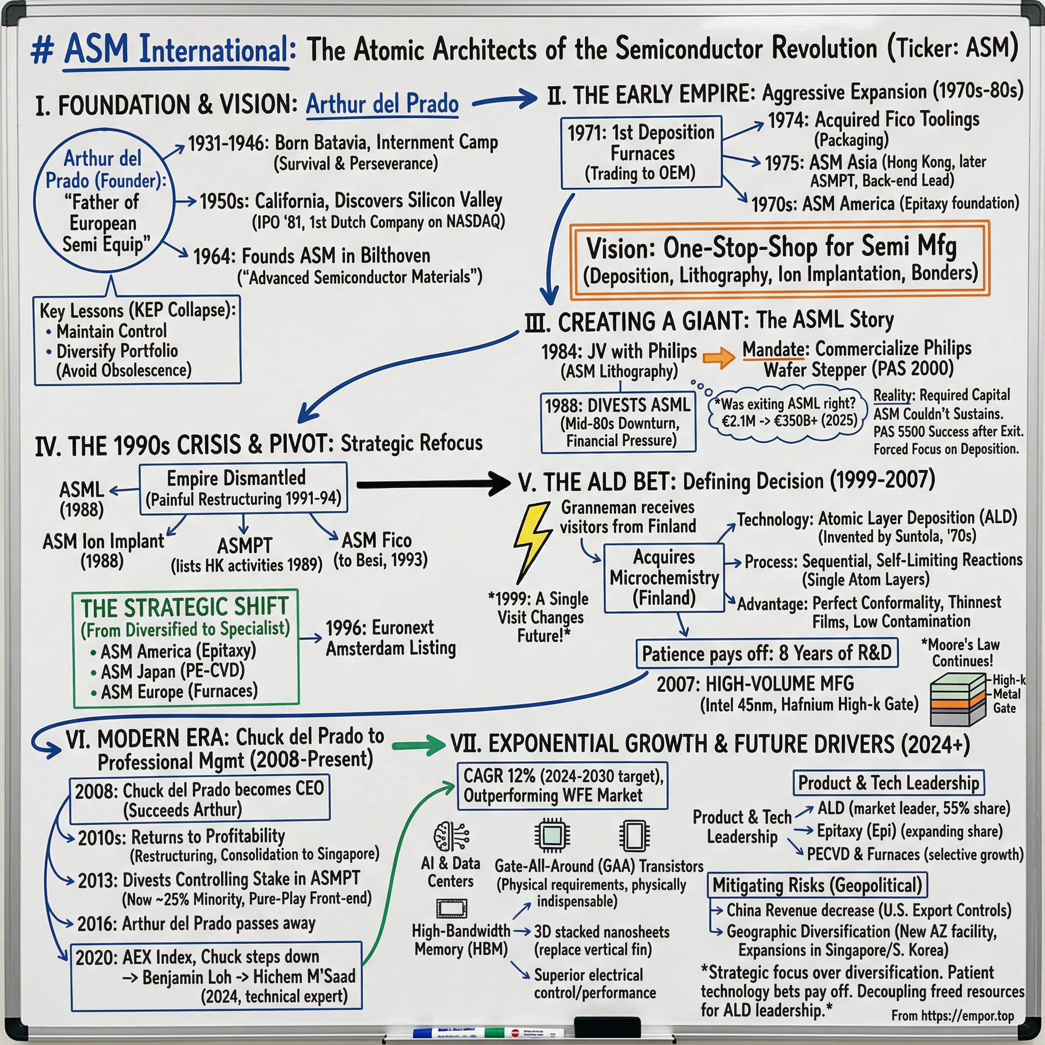
In the sleek fabrication facilities of the world's most advanced chipmakers—TSMC, Samsung, Intel—there exists a technology so precise that it operates at the frontier of what physics allows. Inside machines worth millions of euros, gaseous chemicals pulse through chambers in a carefully choreographed dance, depositing materials onto silicon wafers one atomic layer at a time. The company that dominates this extraordinary niche, commanding over 55% of the single-wafer atomic layer deposition market, is not the industry's most famous name. It is ASM International, a Dutch company headquartered in Almere, with a market capitalization of roughly $27.58 billion—making it the world's 818th most valuable company.
The central question of ASM's story is deceptively simple: How did a small Dutch company, founded by a visionary entrepreneur in a quiet village near Utrecht, become the undisputed leader in the technology that literally builds semiconductors one atom at a time?
ASMI is not just a participant but the undisputed leader, commanding a market share of over 55% in the single-wafer ALD segment. This leadership stems from its first-mover advantage—having pioneered the technology for mass production—and its possession of the industry's broadest portfolio, covering both thermal ALD and plasma-enhanced ALD (PEALD) for different applications.
The answer involves a founder who survived Japanese internment camps in Indonesia, a spinoff that became one of Europe's most valuable companies (ASML, now worth nearly $390 billion), a daring acquisition of a small Finnish company that knew how to deposit exotic materials on semiconductor substrates, and a near-death experience in the 1990s that forced the company to abandon its empire-building ambitions and focus on the atomic frontier.
Semiconductor equipment companies ASML, ASM Pacific Technology (ASMPT) and Besi are former divisions of ASM. Arthur del Prado, ASM's founder, was so prolific that three publicly traded semiconductor equipment companies trace their origins to enterprises he built. Yet unlike empire-builders who hold onto everything, del Prado was forced—sometimes painfully—to let go. The result was a company that traded breadth for depth, diversification for dominance.
Today, ASM International finds itself at another inflection point. This new 3D structure, where the gate material must wrap completely around multiple horizontal nanosheets, presents a geometric challenge of immense complexity. The perfect conformality offered by ALD is no longer just preferred; it becomes a non-negotiable physical requirement for the device to function. For full-year 2024, ASM outperformed the wafer fab equipment market with 12% growth, marking its eighth consecutive year of double-digit growth. The company has delivered eight consecutive years of double-digit revenue growth and is positioned to benefit disproportionately from the industry's transition to gate-all-around transistor architectures.
This is the story of strategic focus triumphing over strategic sprawl, of patient technology bets paying off after nearly a decade of R&D, and of a family business that had to fight hedge funds, survive industry downturns, and repeatedly reinvent itself to become indispensable to the most sophisticated manufacturers on Earth.
II. The Arthur del Prado Story: From Japanese Prison Camp to Silicon Valley
The man who would become known as the "Father of the European Semiconductor Equipment Industry" was born in circumstances that could hardly have been less promising. Del Prado was born on November 17, 1931 in Batavia, the former Dutch Indies (now Jakarta) as the second child of a maritime officer of the 'Royal Packet Navigation Company'. The Del Prado family name originated from Suriname. In 1942, during the Japanese occupation of the Dutch East Indies, like all Dutch citizens, Del Prado was interned together with his mother and older sister in Camp Tjideng, Batavia.
The young Arthur was only eleven years old when his world collapsed. In 1944, all Dutch boys above age 10 were moved to adult camps. Arthur, 12 years old, was separated from his family and sent to a mixed camp for prisoners of war and internments Camp Tjimahi 4. For the next year, the child lived among grown men in the harsh conditions of a Japanese prison camp, learning lessons about survival, perseverance, and the unpredictability of fate that would shape his approach to business for the next seven decades.
During the Bersiap following the capitulation of the Japanese in August 1945, his parents signed Arthur as Cabin boy on MS Oranje for the first repatriation journey after the war to the Netherlands, where he arrived in January 1946. After reunion, he and his family moved to Naarden, the Netherlands.
In the Netherlands, del Prado reinvented himself. Del Prado graduated in chemistry at the Hogere Textielschool Enschede (now Saxion University of Applied Sciences), while serving as chairman of a local student society. After temporarily studying economics at the University of Amsterdam, he migrated to the United States in 1956. In 1957, he started at Harvard Business School, which he did not finish.
What came next defined del Prado's career. Rather than completing his Harvard MBA, he traveled across America, discovering Silicon Valley at the precise moment the semiconductor industry was being born. As ASM's founder and CEO, Del Prado epitomized the emergent and popular entrepreneurial spirit. He was a pioneer in semiconductor equipment who first brought silicon from Silicon Valley to Europe in 1958. He later made waves with an IPO on NASDAQ in 1981 – a first for a Dutch company. Del Prado's vision and perseverance propelled his company to prominence by showcasing the transformative potential of entrepreneurial ventures in high-tech industries.
Del Prado's first foray into semiconductors was through a company called Knapic Electro-Physics (KEP), where he helped sell silicon crystal-growing equipment in Europe. But KEP's collapse taught him two crucial lessons that would guide ASM's strategy for decades. First was that a founder could lose control of their company if it had external investors. Having been responsible for his own success so far, Del Prado was determined to secure maximum elbow room for himself. He would not face Knapic's fate. The second was that it was crucial for a business like KEP to diversify its operations. The rise of float-zone-grown silicon had quickly undermined Knapic's business. An expanded product portfolio formed a hedge against such surprises.
In February 1964, following the liquidation of Knapic Electro-Physics, Arthur del Prado founded Advanced Semiconductor Materials (ASM) as a one-man-business. Initially operating as a sales agent of silicon, he soon expanded into the sale of various American-made technologies used in the production of semiconductors.
The company was founded in Bilthoven, a quiet village in the heart of the Netherlands. In 1964, Arthur del Prado founds ASM as 'Advanced Semiconductor Materials' in Bilthoven, the Netherlands. Initially the company operates as a sales agent in semiconductor fabrication technology in Europe. From this unlikely location, del Prado would build not one but several companies that would reshape the global semiconductor equipment industry.
The European context was crucial. Against the backdrop of the European Commission's novel microelectronics program, ESPRIT, chip companies had voiced concerns about their reliance on American equipment. Responding to industry needs, the Ministry and Arthur Del Prado himself proposed ASM as a potential solution. Del Prado understood that Europe needed its own semiconductor infrastructure, and he was determined to build it.
His personal style was legendary in the industry. From 1960s until his death, Arthur del Prado lived in Bilthoven, the Netherlands. He had three children. His hobbies were amongst others tennis, flying his own airplane, and sailing his own yacht called Skipper. The founder who flew his own plane and sailed his own yacht brought the same fearless confidence to business decisions, even when they seemed foolhardy to outsiders.
Recognized as a visionary for his contributions to the semiconductor equipment industry over the last four decades, particularly in Europe, Arthur del Prado has earned the designation, "Father of the European Semiconductor Equipment Industry." In 2008, he became the first non-American to receive the "Legend of the Industry" award at SEMICON West, the semiconductor industry's premier trade show. In making the presentation, Chad Keck, Needham's Vice Chairman cited Arthur del Prado's vision, leadership, longevity and tenacity as the basis for his being named a legend of the industry.
III. The Early Empire: Building a Diversified Semiconductor Equipment Company
The 1970s marked ASM's transformation from a trading company into an original equipment manufacturer. ASM starts to design, manufacture and sell chemical vapor deposition equipment. In 1971 ASMI launched production of the first vapor deposition furnaces. The company grew from sales to innovation, developing and manufacturing its own technologies.
Del Prado's strategy was aggressive expansion—both geographically and technologically. In 1974 del Prado acquired a controlling stake in Fico Toolings, later ASM Fico, a manufacturer of materials for use in the semiconductor packaging industry. From the 1960s, this part of the industry was mostly located in Southeast Asia. Seeing the trend, in 1975 del Prado opened ASM Asia in Hong Kong.
The global footprint expanded rapidly. As a pioneer of technology advancement and globalization, the company also began launching new companies around the world. In the mid 1970s, ASMPT was founded in Hong Kong, becoming a market leader in back-end semiconductor assembly and packaging equipment. ASM divested its majority share in ASMPT in 2013, but maintains a minority share today. ASM America was also founded in the 1970s, laying the foundation of our current epitaxy technology.
The early 1980s brought a milestone that would prove crucial to ASM's future: the company became the first Dutch company to go public on NASDAQ. Following an initial public offering on the Nasdaq in May 1981, the company expands. In 1982 ASM Japan is established. ASM invests in new semiconductor fabrication technologies, like lithography, ion implantation, epitaxy, and wire bonding.
Del Prado's ambition was nothing less than building a one-stop-shop for semiconductor manufacturing equipment. By the mid-eighties, ASMI's product portfolio included nearly all major semiconductor production technologies: deposition furnaces, lithography, ion implantation, die and wire bonders, and various packaging technologies. It was an audacious vision—and ultimately an unsustainable one.
The most consequential decision of this period came in 1984, when ASM entered into a joint venture with Philips, the Dutch electronics giant, to commercialize lithography technology. This joint venture would become ASML.
IV. The ASML Story: Creating a €350 Billion Giant (Then Letting It Go)
The creation of ASML stands as both Arthur del Prado's greatest entrepreneurial achievement and ASM International's most painful strategic retreat. ASML was established as ASM Lithography on April 1, 1984. The joint venture from Philips and ASM International had a mandate: to commercialize a wafer stepper that had been developed at Philips, the PAS 2000.
The backstory reveals the improbable circumstances that brought two very different Dutch companies together. Advanced Semiconductor Materials International (ASMI) was based in the village of Bilthoven, northeast of Utrecht. ASM was run by Arthur del Prado who had overseen rapid growth in the company's sales and profits. Del Prado had been pushing Elcoma for years to let his firm make more of their production machinery that they use.
Philips executives were initially skeptical. Despite Del Prado's entrepreneurism and success, Philips executives regarded ASM as an upstart. Perkin Elmer – a big, diversified company with a vast installed base of lithography tools – was considered a more robust partner. But ultimately, Troost and other members of Philips management realised that ASMI was their last chance to save the stepper business. They met del Prado again in 1983 and work to hammer out a deal. Del Prado was insistent on one point throughout: that the new company should continue to have access to Natlab's expertise.
The two firms would each own 50% of the new firm – now called ASM Lithographic Systems B.V. – and would each contribute $2.1m to the joint venture.
The joint venture's early years were brutal. In a market of fierce competition and many suppliers, the small unknown company from the Netherlands couldn't catch a break. ASML had few customers and was unable to stand on its own two feet. Making matters worse, shareholder ASMI was unable to maintain the high levels of investment with little return and decided to withdraw, while the global electronics industry took a turn for the worse, and Philips announced a vast cost-cutting program. The life of our young cash-devouring lithography company hung in the balance. Guided by a strong belief in the ongoing R&D and in desperate need of funds, ASML executives reached out to Philips board member Henk Bodt, who persuaded his colleagues to lend a final helping hand.
The timing could not have been worse for ASM. The mid-1980s semiconductor industry downturn created enormous financial pressure. Financial pressures created by a mid-1980s chip industry downturn led ASM to sell its 50 percent ownership of ASML to Philips in 1988.
1984: Royal Philips Electronics and Advanced Semiconductor Materials (later named ASM International) launch ASML as a joint venture. 1988: Company ends joint venture relationship with ASM International. 1993: Company ends joint venture relationship with Royal Philips Electronics.
The question that haunts ASM International's history: Was exiting ASML the right decision?
As of November 2025 ASML has a market cap of $389.39 Billion USD. This makes ASML the world's 27th most valuable company by market cap according to our data. To put this in perspective, ASML is now worth more than 14 times ASM International's current market capitalization.
But the counterfactual requires nuance. ASM was struggling financially and could not sustain the massive capital requirements of developing cutting-edge lithography technology. The investment was put to good use. Within the year, we launched a breakthrough platform, the PAS 5500. With its industry-leading productivity and resolution, the PAS 5500 brought on board the key customers that ASML needed to turn a profit. This breakthrough came after ASM had already exited.
This was followed by ASM's participation in a joint venture with Philips in the mid-1980s to develop lithography technology, known today as ASML. ASM sold its share in ASML in 1988. Since the early 1990s, ASM has focused its efforts on deposition.
The ASML experience taught del Prado and ASM a painful lesson about capital allocation and strategic focus. Sometimes the best decision is to let go—even if what you're letting go becomes spectacularly valuable. The €2.1 million investment that became a €350+ billion company had required resources that ASM simply could not provide while also pursuing its other ambitions.
V. The 1990s Crisis & Strategic Refocus
The late 1980s and early 1990s were years of painful restructuring for ASM International. In 1988, the company divests ASML Holding N.V., ASM Ion Implant, and it lists its Hong Kong–based activities as ASM Pacific Technology on the Hong Kong stock exchange in 1989. The company reorganizes thoroughly between 1991 and 1994. In 1993, ASM divests ASM Fico to Berliner Electro Holding, now known as Besi.
The empire that del Prado had built was being dismantled piece by piece. Ion implantation—gone. Lithography—gone. Packaging—spun off or sold. The diversified conglomerate strategy that had seemed so compelling in the boom years of the early 1980s had become an albatross.
Even though Del Prado's leadership was partially responsible for the company's failings in the late 1980s and early 1990s, he remained ASM's founder, CEO, and majority shareholder. But he was forced to make changes. An interim manager, Ray Friant, was installed as chief operating officer to help with decision making. To turn around the company's fortunes, Friant argued in a report that Del Prado, whom he acknowledged was a "visionary," needed to be complemented by "practical business personnel who are focused on making money each month." Under his and Del Prado's keen eyes, ASM retained its stake in the increasingly profitable ASM Pacific Technology while simultaneously focusing its business around three novel deposition technologies.
The strategic pivot was dramatic. ASM focusses on vertical low-pressure chemical vapor deposition furnaces by ASM Europe, single wafer plasma-enhanced chemical vapor deposition by ASM Japan and single wafer epitaxy by ASM America. From 1996 onwards, the company is also listed on the Euronext, Amsterdam. ASM retains a majority stake in ASM Pacific Technology.
From diversified equipment maker spanning lithography, implantation, deposition, and packaging, ASM emerged from its crisis as a focused deposition specialist. The company retained its stake in ASMPT—a valuable asset that generated cash flow—but its core identity had shifted to deposition: the precise application of thin films to semiconductor wafers.
The Euronext listing in 1996 marked ASM's return to financial stability and European capital markets. The company was smaller, more focused, and ready for the next chapter of its story—one that would be defined by a technology that most industry observers had barely heard of: atomic layer deposition.
VI. The ALD Bet: ASM's Defining Strategic Decision (1999-2007)
If there is a single moment that defines ASM International's modern identity, it occurred on a cold January day in 1999, in the company's headquarters in Bilthoven.
On 22 January 1999, a single visit radically overturned ASM International's future. On that date, ASMI chief technology officer Ernst Granneman received two visitors from Finland: Kari Lampinen and Matti Ervasti. The former was a manager for mergers and acquisitions at a Finnish energy company called Fortum. The latter was a manager of a small subsidiary called Microchemistry, located in Espoo, Finland. Both men visited Bilthoven in order to find out whether ASMI was interested in acquiring Microchemistry and its technology. Their pitch was about atomic layer deposition (ALD), a process developed by the founder of Microchemistry. ALD entails the controlled deposition of films in layers of single atoms. The process enabled the formation of the thinnest films with unprecedented conformity and step coverage while offering low contamination of unwanted impurities.
Atomic layer deposition was invented in Finland in the 1970s by Tuomo Suntola. Tuomo Suntola (born 1943) is a Finnish physicist, inventor, and technology leader. He is best known for his pioneering research in materials science, developing the thin film growth technique called atomic layer deposition. In 1971, Tuomo Suntola earned his PhD in semiconductor physics from the Helsinki University of Technology. After completing his PhD, Suntola made his first industrial development while working at VTT Technical Research Centre of Finland, a thin film humidity sensor "Humicap" for Vaisala Oy, a Finnish company specialized in meteorological instruments. In 1974, Suntola started the development of thin film electroluminescent displays in the Finnish company Instrumentarium Oy.
The technology had been used for decades in flat panel display manufacturing but had not yet broken through into the semiconductor industry. In 1987, Suntola started the development of the ALE technology for new applications like photovoltaic devices and heterogeneous catalysts in Microchemistry Ltd., established for that purpose by the Finnish national oil company Neste Oy. In the 1990s, ALE development in Microchemistry was directed to semiconductor applications and ALE reactors suitable for silicon wafer processing. In 1999, Microchemistry Ltd. and the ALD technology were sold to the Dutch ASM International, a major supplier of semiconductor manufacturing equipment and Microchemistry Ltd. became ASM Microchemistry Oy as ASM's Finnish daughter company. Microchemistry Ltd/ASM Microchemistry Ltd was the only manufacturer of commercial ALD-reactors in the 1990s.
What made ALD attractive for semiconductors was a looming crisis in transistor physics. The most prospective was the gate stack. Microchemistry knew how to use ALD for the deposition of new exotic materials for the gate stack, for instance for the creation of high-k dielectrics and metal electrodes. By 1999, the first alteration of the CMOS gate stack in forty years of semiconductor manufacturing was already looming large on the horizon. It was this application that stirred the interest of chip manufacturers like Intel. Microchemistry's work on gate stack materials also perfectly aligned with ASMI's work done in an earlier European research project and a joint development program with Siemens on integrated deposition processes in multi-chamber systems. Process and material-wise, Microchemistry's techniques formed the missing piece. Moreover, some of its tools were designed according to the industry's Material and Equipment Standards and Code (MESC).
Werkhoven and Granneman visited Microchemistry to learn about the technology. Del Prado, Granneman, and ASMI's CFO Rinse de Jong worked out the financial details with Ervasti and Lampinen. By July, Del Prado and De Jong succeeded in finding "an acceptable creative financial solution" and finalized the acquisition. The firm was now called ASM Microchemistry. In 1999, Microchemistry employed 42 staff, of whom 14 in development, 12 in engineering and 8 in manufacturing. It had four types of machines, including the F120 and the F200 for semiconductor production. The F120 was a mere R&D reactor, only capable of processing very small substrates and primarily meant for process development. The F200 was designed for semiconductor manufacturing. Technology development agreements were in place or were negotiated with Intel and IBM.
ASM had placed its bet on a technology that would not reach high-volume manufacturing for nearly a decade. "In 1999, we acquired the Finnish company Microchemistry, forming ASM Microchemistry. Microchemistry had been researching ALD for catalyst and solar cell applications since 1987. At the same time, new ALD reactor concepts were being studied, with the very first 200 mm wafer processing equipment being designed and built in the late 1990s," it said. "We invested a further 8 years of R&D efforts to design and produce the equipment and processes required to enable its reliable and efficient use by advanced semiconductor chip manufacturers."
The breakthrough came in 2007. In 2007, the company successfully brings atomic layer deposition from R&D to high-volume production via the high-κ metal gate application.
Intel made a significant breakthrough in the 45nm process by using a "high-k" (Hi-k) material called hafnium to replace the transistor's silicon dioxide gate dielectric, and by using new metals to replace the N and PMOS polysilicon gate electrodes. These new materials (along with the right process recipe) reduced the NMOS gate leakage by >25X and PMOS gate leakage by more than 1000X while simultaneously delivering improved drive current and improved circuit performance.
The reduction in gate leakage results from the fact that the gate oxide thickness can be increased using this hafnium-based high-k dielectric, which is produced by atomic layer deposition (ALD).
In 2007, our Pulsar ALD tool became the first system used in the high-volume manufacturing of devices using a new hafnium-based high-k gate dielectric material.
The moment was historic—not just for ASM, but for the entire semiconductor industry. The invention of high-k plus metal gate transistors was an important breakthrough. Although we could have continued to shrink transistors to fit the dimensions needed for the 45-nm generation without this breakthrough, those transistors would not have worked much better than their predecessors, and they certainly would have expended more watts.
The number of reactor manufacturers increased rapidly and semiconductor applications became the industrial breakthrough of the ALD technology, as ALD became an enabling technology for the continuation of Moore's law.
ASM had invested nearly a decade in a technology that had no guaranteed commercial application. The Microchemistry acquisition, the years of process development, the patient engagement with Intel and other leading chipmakers—all of it culminated in 2007 when ALD went from laboratory curiosity to essential manufacturing technology.
In 2004, ASM had further strengthened its ALD position by acquiring Genitech Korea. Recognizing the future of chipmaking lay in ever-thinner and more complex material layers, ASMI divested from other areas to concentrate its resources intensely on deposition technology. This focus was cemented through key acquisitions, notably ASM Microchemistry of Finland in 1999 and Genitech Korea in 2004, which formed the nucleus of its now-dominant ALD business.
VII. The Chuck del Prado Era: Father to Son Transition (2008-2020)
The transition of leadership from Arthur to Chuck del Prado was announced in 2007 and took effect on March 1, 2008. The Boards of ASM International N.V. announced today that Chuck del Prado has been appointed Chief Executive Officer of ASM International, effective March 1, 2008. Chuck del Prado, President and General Manager of ASM America and a member of the Management Board, has been with ASM International since 2001. He will succeed Arthur del Prado, who has served as ASM International's Chief Executive Officer since he founded the Company in the Netherlands in 1968.
An engineer and technology manager, Chuck del Prado (46) has two decades of experience in the computer and semiconductor industries. Prior to joining ASM International as Director of Marketing, Sales and Service of ASM Europe in 2001, he served five years as a manager in sales and manufacturing with ASM Lithography, in Taiwan and the Netherlands. He began his career at IBM Nederland N.V. where he held a variety of sales and global account management positions for more than 7 years. Chuck del Prado received a Master-of-Science degree from the University of Twente in the Netherlands, with a concentration in industrial engineering, computer science and technology management.
The succession was not without controversy. Every son who succeeds his father in the family business has a lot to prove. To himself and his father, but perhaps most of all to the outside world. Even if never said out loud, there always will be suspicions that junior might not have gotten the job if daddy wasn't pulling the strings. Chuck del Prado, however, had his leadership openly questioned almost immediately after he took the helm from his father at ASM International. He had to go all the way to the Dutch Supreme Court to get a chance to prove himself. When we look back at his reign over the company in the past decade, Del Prado was clearly worthy of the job, though.
As President and General Manager of ASM America since 2003, Chuck del Prado has directed the sales, marketing and service of all of ASMI's Front-end product lines to US customers and has led on a global basis the product management, research & development, manufacturing and service of the epitaxy product line and the transistor/capacitor product line, which is based on atomic layer deposition technology including high-k applications.
Chuck del Prado inherited a company that had just achieved its ALD breakthrough but was still struggling with profitability. The years that followed required significant restructuring. 2010s: The company returns to structural profitability after execution of a worldwide restructuring program, that includes the implementation of a product driven organization, a single global sales organization, consolidation of manufacturing in Singapore, and the establishment of a global human resources, finance, IT, operational excellence and environment, health and safety organization.
The application of (plasma enhanced) atomic layer deposition in multiple patterning and high-κ metal gate drives ASM's growth. Other products include epitaxy, PECVD and vertical furnace. Its stake in ASM Pacific Technology is reduced to 25%.
The most significant strategic move of Chuck del Prado's tenure was the divestiture of ASM's controlling stake in ASMPT in 2013. ASMI divested its controlling stake in ASMPT in 2013 and today holds a minority share of approximately 25%, establishing ASMI as a pure-play specialist in front-end wafer fabrication equipment, distinct from ASMPT's focus on the back-end of the chipmaking process.
This decision transformed ASM from a company with significant exposure to back-end assembly and packaging into a pure-play front-end deposition specialist. The strategic rationale was clear: ALD and epitaxy were ASM's areas of technological leadership, and the company needed to focus its resources where it had competitive advantages.
Jan Lobbezoo, Chairman of the Supervisory Board commented: "The Supervisory Board is grateful for the immense contribution of Chuck del Prado to the strong advancement of the company's position in the semiconductor equipment industry. Under Chuck's leadership – and building on the legacy of the late Arthur del Prado - ASM has become a globally leading player in semiconductor equipment, delivering excellent benefits to all stakeholders. The Supervisory Board will be sorry to see Chuck go, but we fully understand and respect his decision. He will leave behind a company that is excellently positioned to continue and further expand its leading position in the semiconductor equipment industry."
Arthur del Prado died on September 9, 2016. Arthur died peacefully at his home on September 9, 2016. He is rightfully recognized as the father of the European semiconductor industry. Indeed it is impossible to imagine today's industry without him. From its onset, more than five decades ago, to the present day, his imprint and influence on the industry has been clear and unmistakable.
VIII. The Modern Era: AI, GAA Transistors & Exponential Growth (2020-Present)
The year 2020 marked multiple transitions for ASM International. In 2020, on the Euronext, the company is included on the AEX index, which includes the top-25 of companies listed on the Euronext Amsterdam stock exchange. The same year, after 12 years as CEO, Chuck del Prado decided to step down, and was succeeded by Benjamin Loh.
He was succeeded by his son, Chuck del Prado, who was CEO until 2020. In May 2024, Hichem M'Saad, our former CTO, was appointed to CEO.
The leadership transition from the del Prado family to professional managers marked the end of an era. Hichem M'Saad, the company's former Chief Technology Officer, brought deep technical expertise to the CEO role—a fitting choice for a company whose competitive advantage rests on atomic-scale precision.
ASM's financial performance in recent years has been exceptional. In 2024, ASM International NV's revenue was 2.93 billion, an increase of 11.33% compared to the previous year's 2.63 billion. Earnings were 685.73 million. For full-year 2024, ASM outperformed the wafer fab equipment market with 12% growth, marking its eighth consecutive year of double-digit growth. Memory sales rebounded from 11% in 2023 to 25% in 2024.
The Q4 2024 results demonstrated continued momentum. New orders of €731 million in Q4 2024 increased YoY by 8% at constant currencies, with the increase again mainly driven by solid demand for gate-all-around (GAA) and high-bandwidth memory (HBM) DRAM. Revenue of €809 million increased by 27% at constant currencies from Q4 of last year.
The company's outlook for 2025 initially appeared strong. We confirm our target for revenue in a range of €3.2-3.6 billion in 2025, but it is too early to provide a more specific forecast due to market uncertainty and as visibility for the second half of the year is still limited.
However, the semiconductor industry's inherent cyclicality has reasserted itself. The Dutch company anticipates second-half revenue will be 5% to 10% lower compared to the first half of 2025 at constant currency rates. It had previously expected revenue in the second half to be flat compared with the first half.
This is due to lower-than-expected demand in leading-edge logic/foundry, with a mixed picture per customer, as well as lower demand in the power/wafer/analog markets. For this reason, revenue in the second half of 2025 is expected to be 5%-10% lower compared to the first half of 2025 at constant currencies. For bookings, the above-mentioned demand weakness is projected to result in a book to bill of below 1 in the second half of 2025.
Despite near-term headwinds, ASM's long-term positioning remains strong. Hichem M'Saad, CEO of ASM, said: "The semiconductor market is on track to reach US$1 trillion by the end of the decade, driven by lasting megatrends, especially AI. The industry's shift to complex 3D architectures and advanced materials aligns perfectly with ASM's strengths, as we support our customers in their relentless pursuit of next-generation devices. We met our strategic targets - holding our leading market share in ALD, growing our share in epitaxy (Epi), and delivering solid, profitable growth, despite mixed market conditions."
The Gate-All-Around Opportunity
The most significant structural tailwind for ASM is the semiconductor industry's transition from FinFET to gate-all-around transistor architectures. After more than a decade of dominance, the FinFET transistor architecture, which powered the smartphone revolution, is reaching its fundamental physical scaling limits. To continue the relentless march of Moore's Law, the semiconductor industry is undertaking its most significant architectural change in a generation: the transition to Gate-All-Around (GAA) transistors. Leading foundries, including Samsung, TSMC, and Intel, are introducing this technology at their most advanced 3nm and 2nm manufacturing nodes. For ASMI, this is not merely a cyclical upgrade; it is a profound, long-term growth accelerant.
To further improve the control of the transistor channel, engineers found a way to replace the vertical fin with a stack of horizontal sheets, creating a new concept called gate-all-around field-effect transistors. Gate-all-around transistors use stacked nanosheets. These separate horizontal sheets are vertically stacked so that the gate surrounds the channel on all four sides, further reducing leakage and increasing drive current. This means superior electrical signals pass through and between the transistors, improving chip performance. Additionally, chipmakers now have the flexibility to vary the width of the nanosheets to best suit a particular chip design.
The geometric complexity of GAA structures, which involve wrapping the transistor gate completely around multiple horizontal nanosheets of silicon, dramatically increases the number of manufacturing steps that require the atomic-level precision and perfect conformality that only ALD can provide.
The transition to the next GAA generation, 1.4nm, is expected to add a further US$450-500 million to our SAM, with the strongest growth in front-end-of-line (FEOL, transistor) applications where ASM holds leadership positions.
The company has set ambitious targets for 2030. Revenue is targeted to increase to more than €5.7 billion by 2030. This implies a 2024-2030 CAGR of at least 12%, compared to a CAGR of 6% for the WFE market over the same period; Gross margin is targeted in a range of 47%-51% (2026-2030).
The single-wafer ALD market is forecasted to increase from US$3.0 billion in 2024 to US$5.1-6.1 billion by 2030, representing a CAGR of 9%-13%. In Epi, we have successfully increased our share in the leading-edge segment and remain focused on further expansion.
Geopolitical and Regulatory Risks
No discussion of ASM's outlook would be complete without addressing China. Taking into account the recently announced new U.S. export controls and as communicated in our press release of December 4, 2024, our China revenue is expected to decrease in 2025, with equipment sales from this market falling in a range of low-to-high 20s percentage of total ASM revenue.
However, China revenue is expected to decrease in 2025 due to new U.S. export controls.
The company is taking steps to mitigate geopolitical risk through geographic diversification of manufacturing. This includes through the construction of a new facility in Scottsdale, Arizona, expected to be completed in the second half of 2026. The company is also enhancing its global supply chain flexibility by expanding manufacturing capacity in Singapore and South Korea.
IX. Technology Deep Dive: How ASM's Products Work
ASM International's competitive advantage rests on a deep understanding of how to deposit extremely thin films of materials onto silicon wafers with atomic precision. The company's product portfolio spans several deposition technologies, but ALD remains the crown jewel.
Atomic layer deposition (ALD) is a thin-film deposition technique based on the sequential use of a gas-phase chemical process; it is a subclass of chemical vapour deposition. The majority of ALD reactions use two chemicals called precursors (also called "reactants"). These precursors react with the surface of a material one at a time in a sequential, self-limiting, manner. A thin film is slowly deposited through repeated exposure to separate precursors. ALD is a key process in fabricating semiconductor devices, and part of the set of tools for synthesizing nanomaterials. During atomic layer deposition, a film is grown on a substrate by exposing its surface to alternate gaseous species (typically referred to as precursors or reactants). In contrast to chemical vapor deposition, the precursors are never present simultaneously in the reactor, but they are inserted as a series of sequential, non-overlapping pulses.
In each of these pulses the precursor molecules react with the surface in a self-limiting way, so that the reaction terminates once all the available sites on the surface are consumed. Consequently, the maximum amount of material deposited on the surface after a single exposure to all of the precursors (a so-called ALD cycle) is determined by the nature of the precursor-surface interaction. By varying the number of cycles it is possible to grow materials uniformly and with high precision on arbitrarily complex and large substrates. ALD is a deposition method with great potential for producing very thin, conformal films with control of the thickness and composition of the films possible at the atomic level. A major driving force for the recent interest is the prospective seen for ALD in scaling down microelectronic devices according to Moore's law.
ASM's products fall into several categories:
Atomic Layer Deposition (ALD): We are market leader in ALD (mid 50s% share). ALD accounts for more than half of our total equipment revenue. The company offers both thermal ALD and plasma-enhanced ALD (PEALD) platforms, with flagship products including the Eagle XP8 for metal ALD applications and the Pulsar platform that enabled the high-k metal gate breakthrough.
Epitaxy (Epi): ASMI holds a global market share exceeding 55% in ALD equipment supply. ASMI is also expanding into adjacent deposition technologies, such as silicon epitaxy, and is expected to achieve a 30% global market share in this area by 2025.
PECVD and Vertical Furnaces: ASM also offers plasma-enhanced chemical vapor deposition and batch vertical furnace systems, though these represent selective growth areas rather than the company's primary focus.
Silicon Carbide Epitaxy: In SiC Epi, the outlook further weakened. This segment, which serves the power semiconductor market, has faced headwinds due to cyclical corrections in automotive and power applications.
The technology roadmap extends into increasingly complex architectures. ALD intensity is rising as leading-edge nodes (2 nm and 1.4 nm) require more deposition steps for complex 3D structures, high-k dielectrics, and metal gate stacks. ASM confirmed ongoing R&D engagement for 1.4nm and highlighted that ALD demand will further accelerate in next-gen nodes, backside power delivery, and in advanced DRAM (e.g. HBM), which increasingly adopt logic-like ALD layers.
X. Playbook: Business & Investing Lessons
Strategic Focus Over Diversification
ASM's journey from diversified equipment conglomerate to pure-play deposition specialist offers a powerful lesson in strategic focus. Arthur del Prado's original vision—a one-stop-shop spanning lithography, implantation, deposition, and packaging—proved unsustainable. The company couldn't compete effectively across so many technology domains simultaneously.
The painful restructuring of the 1990s forced ASM to make hard choices. By focusing on deposition—and specifically on ALD—the company created a dominant position in a critical niche rather than a marginal presence across many segments.
The Power of Patient Technology Bets
The 1999 Microchemistry acquisition exemplifies patient capital allocation. ASM invested in ALD technology that would not reach high-volume manufacturing for nearly a decade. Most corporate executives operating under quarterly earnings pressure would never have made such a bet.
The Finnish process pioneered at Microchemistry proved to be critical in the deposition of exotic materials, such as hafnium oxide, onto increasingly complex transistor geometries. Along with the company's well-established business groups in vertical furnaces, epitaxy, and plasma deposition, the new market in atomic layer deposition helped ASM enjoy success in the 2010s.
Knowing When to Divest
ASM's history is littered with divestitures: ASML, Ion Implant, ASM Fico (now Besi), and the majority stake in ASMPT. Each divestiture was painful at the time—especially ASML, which became spectacularly valuable—but each also freed resources for the company's areas of genuine competitive advantage.
The ASMPT divestiture in 2013 transformed ASM into a pure-play front-end specialist. The cash generated from selling down that stake funded the company's growth in ALD and epitaxy.
Family Business Dynamics
The transition from Arthur to Chuck del Prado, and eventually to professional management, demonstrates both the strengths and limitations of family business succession. Arthur's vision and risk tolerance built the company; Chuck's operational discipline restored profitability and executed the strategic focus. The subsequent transition to non-family management (Benjamin Loh, then Hichem M'Saad) brought deep technical expertise appropriate for a technology-driven company.
XI. The Competitive Landscape and Moat Analysis
Porter's Five Forces Assessment
Threat of New Entrants: Low to Moderate
The technical barriers to entry for competitors grow higher, as the process window for successful deposition becomes vanishingly small. ALD requires decades of accumulated process knowledge, proprietary reactor designs, and deep customer relationships. However, Chinese equipment makers backed by government subsidies represent a long-term threat in less-advanced applications.
Bargaining Power of Suppliers: Moderate
ASM relies on specialized precursor chemicals and components. The supply chain for advanced semiconductor equipment is complex but manageable for a company of ASM's scale.
Bargaining Power of Buyers: High
In 2024, the top five customers accounted for approximately 51% of its revenue, and the potential loss of larger individual customers poses a material risk. Customer concentration is significant, with TSMC, Samsung, Intel, SK hynix, and Micron likely representing the bulk of revenue.
Threat of Substitutes: Low
For the most demanding applications—high-k metal gate, GAA transistors, HBM DRAM—no alternative deposition technology can match ALD's precision. CVD and PVD lack the conformality required for advanced 3D structures.
Competitive Rivalry: Moderate to High
ASM faces direct competition from Applied Materials (AMAT), Tokyo Electron (TEL) and Lam Research in ALD and epi; price pressure in batch ALD and hybrid tool strategies are potential margin headwinds.
Hamilton Helmer's 7 Powers Framework
Process Power: ASM's two decades of ALD process development have created embedded learning advantages that competitors cannot easily replicate. The company's reactor technology and process recipes represent accumulated intellectual property.
Switching Costs: This technological leadership translates into a powerful economic advantage through high switching costs. When a leading chipmaker like TSMC, Samsung, or Intel develops a process for a new manufacturing node—for instance, their 2-nanometer process—they spend years and billions of dollars qualifying specific tools and materials.
Scale Economies: ASM's scale in ALD allows for efficient R&D spending and manufacturing operations, though it is smaller than diversified competitors like Applied Materials.
Cornered Resource: The company's heritage in ALD—including the Finnish research team, patent portfolio, and customer relationships—represents a cornered resource that competitors cannot easily acquire.
Counter-Positioning: ASM's pure-play focus on deposition differs from larger competitors who must spread resources across multiple equipment categories.
Competitive Positioning
ASM's top 3 competitors are Applied Materials, Lam Research, TEL. Applied Materials is the most similar to ASM. Lam Research and TEL are also similar to ASM.
Applied Materials: broad WFE scale; AMAT's 2024 acquisition of Picosun strengthened low‑temp ALD, increasing pressure on specialty ALD segments. Lam Research: integrated PEALD + etch gives process lock‑in; benefited from 3D NAND demand. Tokyo Electron: strong regional penetration; deep service footprint in Japan/Korea. Kokusai: batch ALD cost advantage for high‑throughput layers.
ASM's competitive moat rests on its leadership in single-wafer ALD for the most demanding applications. While competitors can serve less-advanced segments, ASM's position at the leading edge—where conformality and precision requirements are most stringent—provides pricing power and margin protection.
XII. Key Metrics for Investors
For investors tracking ASM International, three key performance indicators warrant close attention:
1. ALD Equipment Revenue Growth
ALD represents over half of ASM's equipment revenue and is the company's primary growth engine. Tracking year-over-year growth in ALD equipment sales provides visibility into the company's success in capturing the GAA transition opportunity.
2. Gross Margin
We strive for healthy gross margins of 46%-50% and operating margins of 26-31% in the 2022-2027 period. The company achieved an adjusted gross margin of 50.3% and operating margin of 28.1% in Q4.
Gross margin reflects ASM's pricing power and product mix. A sustained gross margin above 50% indicates strong demand for the company's most advanced (and highest-margin) ALD products. Margin compression would signal intensifying competition or a shift toward lower-value applications.
3. GAA-Related Orders
While recently announced capex reductions have somewhat impacted the outlook for advanced logic/foundry spending, we still project a substantial increase in our GAA-related sales in 2025.
GAA-related orders serve as a leading indicator of ASM's participation in the industry's most significant architectural transition. The timing and magnitude of GAA orders from TSMC, Samsung, and Intel will determine whether ASM can achieve its ambitious 2030 revenue targets.
XIII. Risk Factors and Regulatory Considerations
Customer Concentration
The company's FY24 revenue profile shows that its top five customers accounted for 51% of sales, while the top ten represented 70%, indicating strong relationships with leading-edge semiconductor manufacturers.
This concentration creates meaningful risk. The loss of a single large customer, or a significant reduction in that customer's capital spending, would materially impact ASM's financial results.
Geopolitical and Export Control Risk
Taking into account the recently announced new U.S. export controls, our China revenue is expected to decrease in 2025, with equipment sales from this market falling in a range of low-to-high 20s percentage of total ASM revenue.
Export controls on advanced semiconductor technology have already impacted ASM's China revenue. Further restrictions could reduce the addressable market, though ASM's focus on leading-edge technology (which faces the strictest controls) means it has less exposure to mature-node Chinese demand than some competitors.
Cyclical Exposure
The semiconductor equipment industry is notoriously cyclical. The power/analog/wafer segments are still in a cyclical correction with no signs of a recovery in the near term. ASM's exposure to leading-edge logic and foundry provides some insulation from broader industry cycles, but the company is not immune to capital spending fluctuations.
Competitive Threats
However, the entry of new competitors and the emergence of substitute deposition technologies could hinder ASMI's growth in the long term.
Applied Materials' acquisition of Picosun in 2024 demonstrated that well-capitalized competitors are targeting ASM's ALD leadership. Chinese domestic equipment makers, while currently focused on mature nodes, represent a long-term competitive threat.
XIV. Conclusion: The Atomic Future
ASM International's story is one of reinvention. From Arthur del Prado's one-man operation in Bilthoven to a focused deposition specialist commanding over half the global ALD market, the company has repeatedly transformed itself in response to industry shifts and competitive pressures.
The decisions that shaped ASM's present position—exiting ASML, acquiring Microchemistry, divesting ASMPT, focusing on ALD—seemed risky or even foolhardy at the time. In retrospect, they created a company perfectly positioned for the semiconductor industry's most demanding applications.
This shift fundamentally deepens ASMI's moat, moving the company from a preferred supplier to an indispensable partner for its most important customers and strengthening its long-term pricing power and margin profile.
The gate-all-around transition represents the largest architectural change in transistor design since the FinFET revolution of 2012. ASM's atomic layer deposition technology is not merely helpful for manufacturing GAA transistors—it is physically indispensable. The geometric complexity of wrapping gate material around horizontal nanosheets on all four sides cannot be achieved without the atomic-level precision that ALD provides.
For long-term investors, ASM offers exposure to a critical enabling technology for advanced semiconductor manufacturing. The company's dominant market share, high switching costs, and expanding addressable market create a compelling structural position. The risks—customer concentration, geopolitical uncertainty, and competitive threats—are real but manageable for a company with ASM's technological leadership and customer relationships.
Arthur del Prado, who survived Japanese internment camps to become the father of European semiconductor equipment, would likely appreciate the irony. The company he built by empire-building became great by empire-shedding. The diversified conglomerate that tried to do everything became the focused specialist that does one thing better than anyone else: building semiconductors one atom at a time.
Myth vs. Reality: "ASM Made a Mistake by Selling ASML"
The Myth: ASM's exit from ASML in 1988 was a catastrophic strategic error. ASML is now worth nearly $400 billion—ASM could have owned half of that.
The Reality: The counterfactual ignores critical context. ASM was financially stressed in 1988 and could not sustain the capital requirements of lithography development. The breakthrough PAS 5500 platform that made ASML successful came after ASM's exit and required investments ASM could not have made while pursuing its other ambitions. More importantly, the exit forced ASM to focus on deposition—creating the strategic clarity that enabled its ALD leadership today. Sometimes the best decision is to let go.
Legal and Regulatory Note: ASM International is subject to export control regulations that limit its ability to sell certain equipment to China. The company has disclosed that these restrictions will reduce China revenue as a percentage of total sales in 2025. Investors should monitor regulatory developments carefully as export controls continue to evolve.
 RSS Feed
 Spotify
 Apple Podcasts
 Amazon Music
 Audible
 YouTube