Dai Nippon Printing: From Meiji-Era Ink to Semiconductor Photomasks
I. Introduction: The Printing Company That Stopped Printing
What if the world’s largest printing company barely did any printing anymore?
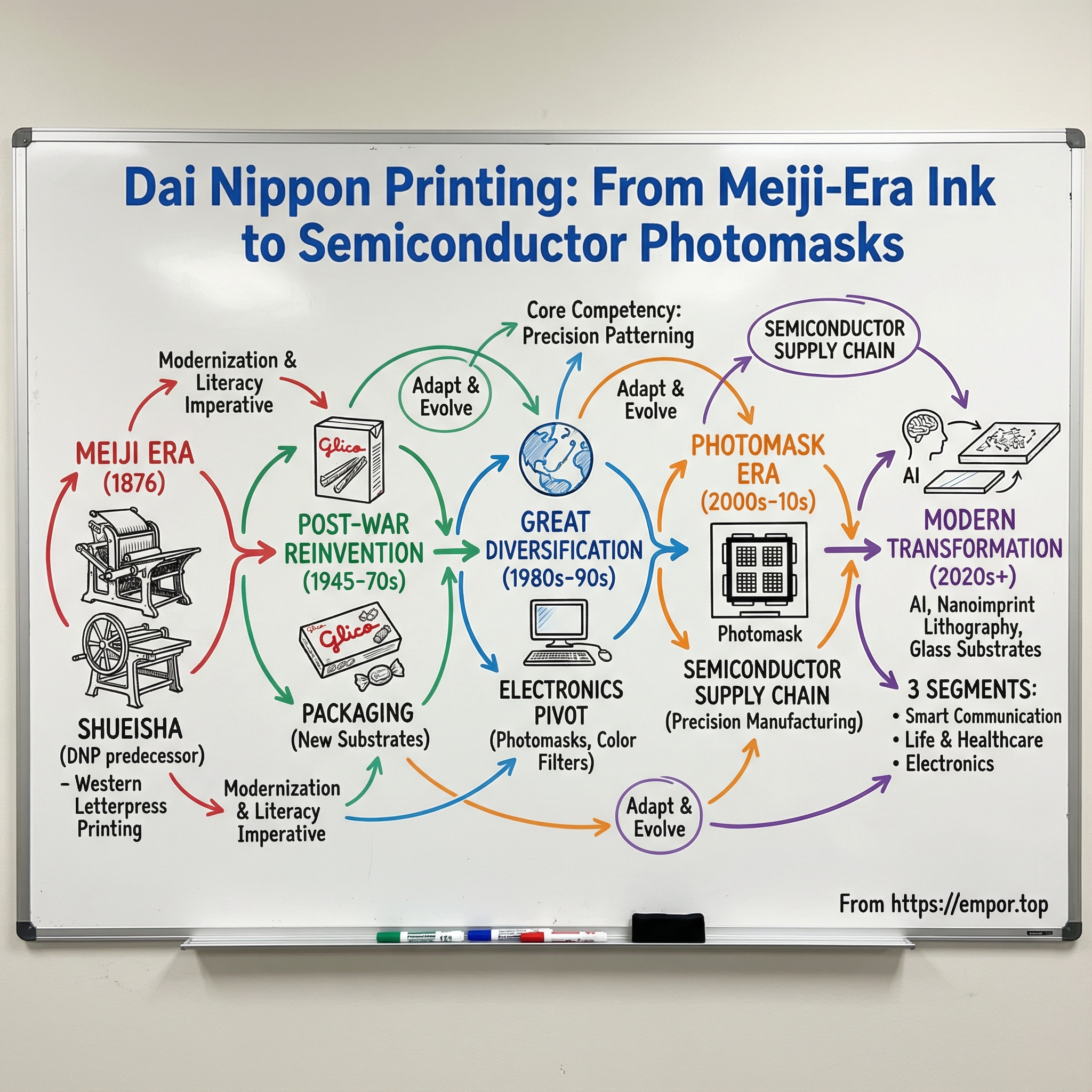
Start in Tokyo in 1876. Japan has just emerged from two centuries of isolation. The Meiji Restoration is still fresh, and the country is sprinting to modernize—laws, schools, industry, everything. In that moment, in a small workshop, a group of entrepreneurs takes a bet on something most people in Japan have barely seen: Western-style letterpress printing. This isn’t just a business plan. It’s a mission. If Japan is going to catch up to the West, it needs mass literacy, mass information, and the ability to reproduce ideas at scale.
That company was Shūeisha, founded in Tokyo the same year. It would later become Dai Nippon Printing Co., Ltd.—DNP. From the beginning, the point wasn’t simply to sell ink on paper. The founders believed printing could raise the knowledge and culture of an entire nation.
Fast-forward nearly a century and a half, and DNP has pulled off something rare: it stayed essential by refusing to stay the same. Japan’s first modern printing company went on to become the largest printing company in the world—and then, quietly, it outgrew the very category that made it famous.
Today, DNP still prints. But “printing company” barely captures what it is. It operates across commercial printing and publishing, yes—but also packaging, decorative interior materials, business forms, and, increasingly, electronics and information technology. It’s built capabilities in precision manufacturing that show up in places you’d never associate with magazines or books: display components like color filters, precision parts, and semiconductor-related components.
That’s the paradox at the heart of DNP. Hear the name “Dai Nippon Printing,” and you picture presses and paper. In reality, the business sprawls across fields that don’t fit neatly under any single label.
In the modern company, those businesses are organized into three segments—Smart Communication, Life & Healthcare, and Electronics. Under that umbrella sits an eclectic but telling catalog: magazines and pamphlets alongside packaging materials; functional films and industrial materials alongside smart cards; battery pouches for lithium-ion batteries; decorative surface materials for buildings; and semiconductor-related components.
DNP now employs close to 40,000 people across Asia, Europe, and North America, and it trades on the Tokyo Stock Exchange as TYO:7912.
This is the story of how a 149-year-old printing company became indispensable to the semiconductor industry—a journey from hand-set movable type to nanometer-scale photomasks that help make the world’s most advanced chips.
II. The Meiji Miracle: Birth of Modern Japanese Printing (1876–1935)
Setting the Scene: Japan's Modernization Imperative
Tokyo, 1876. Japan was reinventing itself in real time.
The Tokugawa shogunate had fallen less than a decade earlier. With it went the national isolation policy that had shaped the country since the 1600s. The Meiji government was opening the doors to Western technology, institutions, and ideas—fast—because the stakes were obvious. Japan had watched what happened to China as foreign powers pressed in. Modernize, or be modernized by someone else.
And in a country trying to build a modern state, information wasn’t a luxury. It was infrastructure. Newspapers to connect a national public. Textbooks to educate a new workforce. Documents to run courts, ministries, and commerce.
The bottleneck was production. Traditional woodblock printing was gorgeous, but it wasn’t built for speed or scale. The new Japan needed pages by the thousands, not by the artisan’s pace.
That’s the opening DNP’s predecessor stepped into. Shūeisha was founded in Tokyo in 1876, right as Japan’s modernization push began accelerating. Demand for printed material surged, and Shūeisha grew with it. It was the only modern Western-style printing firm in Japan at the time, which meant it landed much of the metropolitan newspaper work—its competition mostly small shops still relying on woodblocks.
The Founding Vision: Culture Through Technology
Shūeisha wasn’t launched as a cynical grab for a new market. Its founders talked about printing the way reformers talked about schools: as a way to raise the level of knowledge and culture.
That philosophy showed up immediately in the company’s first major job: printing a revised Japanese translation of Samuel Smiles’ Self-Help.
This wasn’t just another title on a list. Self-Help became a bestseller and gave voice to something Meiji Japan was hungry for—personal initiative, self-improvement, the belief that people could reshape their lives through effort. And Shūeisha didn’t just print the pages; it even developed the paperboard for the cover. It was the first Western-style book made entirely in Japan, end to end.
For a young printing company, it was a statement: we can manufacture modernity here.
First-Mover Advantage and Relentless Innovation
Being early gave Shūeisha a head start. Staying ahead required a different skill: the willingness to keep upgrading while the whole country was upgrading around you.
At first, Shūeisha printed movable type by hand. But in 1884, it installed a steam motor to power its presses—making it the first private company in Japan to use steam power. That shift wasn’t cosmetic. It was a fundamental change in throughput and consistency, and it signaled that printing in Japan was becoming industrial.
From there, the arms race continued—new techniques, better equipment, more capacity—as Japan’s broader papermaking and publishing ecosystem took off. The numbers tell the story of that takeoff: paper production went from tiny in the 1870s to millions of pounds a decade later, and tens of millions by the 1890s. The market was exploding, and Shūeisha was positioning itself to serve it.
In 1886, the company built a factory in Tokyo’s Ichigaya district. And in 1923, after the Great Kantō Earthquake tore through the capital, Shūeisha consolidated its head office functions in Ichigaya as part of regrouping and stabilizing operations.
The One-Yen Book Boom and Market Turmoil
Then came a wave that looked, at first, like a gift: the late-1920s “one-yen book boom.”
Cheap collections of literary works hit the market and found a massive audience. For printers, it meant volume—huge runs, tight schedules, constant demand. Japan was getting its first taste of true mass-market publishing.
But the logic of booms is cruel. When everyone expands to meet surging demand, the industry ends up with too much capacity the moment the surge fades. After the initial frenzy, printing turned into a knife fight—too many firms chasing too few good jobs, pushing prices down just as the global depression made everything harder.
The Merger That Created a Giant
In 1935, Shūeisha made its decisive move. It merged with Nisshin Printing Co., Ltd., and Dai Nippon Printing Co., Ltd.—DNP—was born.
It was a fresh start and a survival strategy at the same time. Consolidation pressure was rising, and scale mattered more than ever. Shūeisha brought technical strength and deep relationships in publishing; Nisshin added capabilities and capacity. Together, they formed the core of what would become Japan’s—and eventually the world’s—largest comprehensive printing company.
DNP would later list shares on the Tokyo Stock Exchange in 1949. But before that future could arrive, history intervened. A world war was coming—one that would devastate Japan’s cities and industry, and force this newly christened company to reinvent itself all over again.
III. Post-War Reinvention: From Books to Boxes (1945–1970s)
The Great Pivot: Why Packaging Changed Everything
When the guns fell silent in August 1945, Japan was shattered. Hiroshima and Nagasaki had been obliterated. Tokyo had been burned down. Industry, logistics, and everyday commerce were broken—and DNP’s presses didn’t escape the wreckage.
Up to that point, DNP was, in a very literal sense, a publishing printer. Until World War II, its business was publications—books, magazines, newspapers. But in the postwar economy, simply returning to the old playbook wasn’t a plan. It was a hope.
So DNP faced an uncomfortable, existential question: after seventy years of getting incredibly good at ink on paper, what do you do when the world around you needs something else?
The first answer didn’t come from a ministry or a boardroom strategy session. It came from a candy company that needed boxes.
The Glico Story: How Candy Boxes Sparked a Transformation
Soon after the war, Ezaki Glico—the confectionery maker known for caramel candies—had a very practical problem. They needed red paper boxes for their products, and postwar Japan couldn’t reliably supply them.
Glico asked DNP if it could deliver.
DNP said yes, then figured out how to make it work with what it had. The boxes shipped, the relationship held, and what looked like a small contract turned out to be a glimpse of the future. Packaging was demand you could feel immediately in a rebuilding economy: consumer goods returning to shelves, brands competing for attention, products needing protection and presentation.
And packaging, in DNP’s eyes, was still “printing”—just printed information and design on a different substrate, serving a different customer, in a different market. That one order became a model: take core printing capabilities, apply them to a new need, and grow outward.
The American Supermarket Insight
In 1950, Orie Kitajima—a DNP director who would later become president and chairman—went to the United States on a study trip. What he saw there reframed the opportunity.
American supermarkets were unlike the retail Japan was used to. Instead of shopkeepers selling from behind a counter, the store itself was designed for self-service. Products sat out in the open, competing side by side. In that environment, packaging wasn’t an afterthought. It was the salesperson. The box had to explain the product, signal quality, and pull you off the shelf—all without anyone saying a word.
Kitajima came home convinced that Japan would move in the same direction, and that packaging would become central to modern consumer life. That insight fed directly into DNP’s first five-year restructuring plan in 1951.
For the first time in its 75-year history, DNP had an official plan that called for expansion beyond publications. The pivot had a name, a timeline, and leadership conviction behind it.
Going Global: The Hong Kong Gambit
While DNP was learning to think like a packaging company, it was also learning to think like a global one.
By the early 1960s, U.S. publishers had started to notice something: Japanese printers could deliver quality work at significantly lower cost than printing at home. DNP leaned into that gap. In 1964, it built a plant in Hong Kong, aimed largely at printing for U.S. publishers—who were paying roughly half of what comparable work cost in the United States.
The strategy was straightforward: keep standards high, move labor-intensive production to a lower-cost base, and invest in world-class equipment. DNP outfitted the Hong Kong facility with modern European presses. The plant focused first on offset printing, particularly color work. And DNP didn’t just hire operators; it built a pipeline, creating an apprenticeship program that sent young Chinese technicians to Japan for training.
That one factory—alongside a similar move by rival Toppan in 1962—became a seed crystal for an entire industry. Hong Kong’s printing sector grew around these capabilities, and by the late 1980s it rivaled Japan’s.
DNP kept pushing outward. In 1968, it opened offices in New York and Düsseldorf to promote its printing and binding internationally.
By the end of the 1960s, DNP no longer looked like a Tokyo publishing printer. It was becoming a multinational manufacturing and services company—printing publications, yes, but also making packaging, expanding overseas, and building the organizational muscle to operate far from home.
And that postwar reinvention set up the next one. Because once you’ve trained yourself to apply “printing” skills to entirely new substrates and markets, the leap from paperboard to electronics starts to look less like a detour—and more like destiny.
IV. The Great Diversification: Electronics Enter the Picture (1980s–1990s)
The Existential Threat: Word Processors and Laser Printers
By the early 1980s, commercial printing was staring down a disruption that, a decade earlier, would’ve sounded absurd: people were going to start doing the printing themselves.
In 1980, Japanese-language word processors arrived, and electronic publishing suddenly became practical in Japan. Over the rest of the decade, computers and word-processing software got cheaper and more common. Then laser printers showed up in offices big and small. By the end of the 1980s, even a modest business could produce its own internal documents, simple brochures, letterheads, and forms.
That wasn’t just competition on price. It was whole categories of work evaporating. The everyday jobs that kept presses running were moving onto desks. For DNP—and for rivals like Toppan—the question wasn’t whether this would hurt. It was how much of the old business would be left when the dust settled.
The logical response was to move closer to where information was headed: into information processing.
The Philosophical Reframing That Enabled Reinvention
Most incumbents react to disruption by defending the perimeter. DNP did something more useful: it changed the definition of what it was.
Inside the company, the argument was simple and surprisingly modern. Printing, they believed, was the first information processing industry. If your job is to take information and reproduce it accurately at scale, then the computer age isn’t the end of printing—it’s the next chapter.
That view wasn’t unique to DNP. Many competitors shared it, and Japan’s Ministry of International Trade and Industry reinforced the framing through the Industrial Structural Council’s Paper and Printing Committee.
Once you accept that identity—information processing, not ink on paper—new businesses stop looking like “diversification” and start looking like adjacent territory. Photomasks for semiconductors. Components for displays. Digital media distribution. It all fits.
The Electronics Pivot: From Ink to Integrated Circuits
DNP’s advantage wasn’t that it could run presses. It was that it could manufacture precision patterns reliably—over and over, at scale.
That skill had been built through decades of plate making and high-resolution printing: controlling materials, coatings, alignment, and defects. Change the substrate and the materials, and the underlying discipline starts to rhyme with electronics manufacturing.
By the 1980s, DNP was deepening relationships with electronics makers, and those ties began to turn into real strategy. In 1990, the company sharpened its overseas focus and marketed photomasks through a partnership with Du Pont Photomask. It also increased its stake in Tien Wah Press in Singapore—eventually taking control—which made Singapore its largest overseas printing base and a key hub for Southeast Asia.
At the same time, DNP pushed into new categories that looked nothing like books and magazines. It entered the global market for projected-television screens, producing in Japan and at the Denmark plant of a new subsidiary, DNP DENMARK. That subsidiary later acquired another Danish company, Scan Screen.
And as the “information processing” thesis kept expanding, so did the tools. DNP began using satellites to move data from its Tokyo headquarters and to distribute business-oriented television programs as part of its audiovisual systems work. It established a Multimedia Communications Center focused on then-cutting-edge formats like HDTV, videodisks, and CD-ROMs.
This wasn’t a single pivot. It was a broad repositioning: away from being a company that printed things, and toward being a company that helped information move—whether that information ended up on paper, on a screen, or etched into silicon.
The Information Media Supplies Division: Betting on Digital
One of the clearest expressions of that strategy showed up in a product most people never think about: thermal transfer ribbons.
In the early 1980s, DNP was an early mover in thermal transfer ribbon technology. The business was a perfect match for what DNP already knew how to do—precision coating and high-reliability manufacturing—and it sat right in the slipstream of digitization. As barcodes spread, industrial labeling exploded, and specialized printing moved into offices and factories, the humble ribbon became a quiet consumable behind a lot of modern logistics.
Years later, in 2008, DNP merged this business with Sony Chemicals’ thermal transfer ribbon division, and DNP’s Imaging Communication subsidiary was founded. Over time, DNP grew into the world’s largest manufacturer of thermal transfer ribbons for barcode and dye-sublimation printers.
The playbook was becoming consistent: find a growing market that rewards precision manufacturing, apply DNP’s process control and scale, and build an unglamorous but defensible position.
The Bid-Rigging Scandal: A Brush with Disgrace
Not everything in the 1990s was a clean upward line.
In late 1992, DNP took a reputational hit when top executives Norio Mizunoya and Tadashi Takehara were implicated in an illegal scheme—along with four other companies, including Toppan Printing—to fix bids on central government contracts.
Japan had long been seen as relatively lenient on antitrust enforcement. But the political winds were shifting, in part because foreign companies—especially American ones—were pushing hard against what they viewed as closed, collusive markets. The government crackdown signaled that the old “everybody understands how this works” approach could now bring real consequences.
The scandal also underlined something else: traditional printing had become brutally competitive, with incentives that could tempt even major incumbents into bad decisions. Against that backdrop, DNP’s move into electronics and information-related businesses didn’t just look forward-thinking. It looked necessary.
By the mid-1990s, DNP appeared to have weathered the damage and returned to steady increases in sales and profit, even in a strained Japanese business climate. The bets that had looked speculative a decade earlier were starting to harden into a new center of gravity for the company.
V. The Photomask Era: DNP's Hidden Semiconductor Empire (2000s–2010s)
Understanding the Photomask Business
To understand how a printing company became indispensable to the semiconductor industry, you first need to understand what a photomask is.
A photomask is a high-precision quartz plate that carries microscopic images of electronic circuit patterns. In chipmaking and flat panel display manufacturing, it’s the master template used to transfer those patterns onto silicon wafers or display substrates during fabrication.
The easiest mental model is a stencil. But it’s a stencil built for a world where “close enough” doesn’t exist. The patterns must be accurate at nanometer scale, the surface must be extraordinarily flat, and a single defect or speck of contamination can spoil an entire run downstream—turning into lost yield, wasted time, and enormous cost.
That combination—precision patterning, ultra-clean materials, ruthless defect control—is exactly the kind of manufacturing discipline DNP had been quietly building for decades.
Why Printing Expertise Translated to Semiconductors
By this point, DNP’s electronics portfolio already included color filters and other LCD components, photomasks, and a range of semiconductor-related products. In photomasks specifically, DNP became a world leader by applying time-honored printing techniques and know-how to the demands of cutting-edge semiconductor manufacturing.
The connection sounds surprising until you look at the underlying work. Traditional printing and photomask fabrication share the same fundamental requirements:
- Precision pattern transfer: reproducing intricate designs faithfully, every time
- Material purity: keeping surfaces clean and contamination-free
- Process control: managing complex, tightly tuned manufacturing steps with consistency
- Inspection and quality assurance: finding defects far smaller than the human eye can see
DNP’s roots in plate-making mattered here. In commercial printing, a tiny flaw can ruin an entire job. That mindset—obsess over surfaces, control variables, catch defects early—translates cleanly to the photomask world, where the stakes are much higher and the tolerances much tighter.
The Battle with Toppan for Photomask Supremacy
For a time, DNP led the photomask market by share. That changed in 2005, when rival Toppan Printing completed the roughly $650 million acquisition of U.S.-based DuPont Photomasks. Overnight, the combined business—Toppan Photomasks—jumped ahead.
“In 2005, Toppan led the worldwide merchant market with a 40.1 percent share after its acquisition of DuPont Photomasks. DNP followed with a 31.8 percent share,” said Robert Castellano, president of The Information Network, in a statement.
The logic of the deal was clear: scale and footprint. DuPont Photomasks brought facilities across Asia, Europe, and the Americas, giving Toppan one of the broadest production networks in the world.
DNP, meanwhile, didn’t respond by trying to win a bidding war. It doubled down on strategy it knew well: partnerships, positioning, and technology.
Strategic Alliances: The Photronics Taiwan Joint Venture (2014)
In 2014, DNP and Photronics closed a joint venture: Photronics DNP Mask Corporation (PDMC). The goal was straightforward and ambitious—serve semiconductor manufacturers in Taiwan, the most important geography in the global chip supply chain. The joint venture followed regulatory approvals from Taiwan authorities on March 28, 2014, and became effective on April 4, 2014.
Photronics’ chairman and CEO framed the pitch in customer terms: “This combination of strengths in logic and memory photomask technology, leveraged by our highly efficient operating model and investment strategy, will provide a superior long-term capability for our customers in the region. In fact, this combination of resources and capability creates the largest domestic supplier of leading edge photomasks in Taiwan with the scale to address 14 nm and beyond technology.”
The subtext mattered as much as the quote. Taiwan wasn’t just another market. It was where the world’s most demanding customers were setting the pace for advanced manufacturing. With PDMC, DNP wasn’t watching the semiconductor industry from the sidelines—it was placing capacity and capability right at the center of it.
The partnership didn’t stop there. With expectations that China would account for a meaningful share of global production capacity by 2020, DNP and Photronics aimed to meet demand from Chinese semiconductor makers for shorter lead times and more stable supply through localized production. In May 2017, they announced plans to establish a China-based joint venture for the manufacture and sales of semiconductor photomasks, and later completed the formal steps to set it up and move into preparation for local production.
It was the same play, repeated with purpose: go where chips are being made, embed yourself in the ecosystem, and become the supplier customers can’t afford to lose.
VI. The Modern Transformation: Semiconductors, AI, and Next-Gen Tech (2020s–Present)
The Current Business Architecture
Modern DNP barely resembles the Meiji-era printer that started in Tokyo in 1876—except for the trait that mattered most: an obsession with precision, quality, and getting better every year.
Today, Dai Nippon Printing operates by applying printing and information technologies across three segments: Smart Communication, Life & Healthcare, and Electronics.
Smart Communication is the biggest revenue engine. It spans imaging communication (including photo printing), Information Security (including BPO and smart card services), and content and XR communication. Life & Healthcare covers mobility and industrial high-performance materials, bulk pharmaceutical manufacturing and medical packaging, plus packaging, living spaces, and beverages. Electronics is where DNP’s “printing turned precision manufacturing” story shows up most clearly: functional films, display components, and other electronics-related products.
In the fiscal year ended March 2024, DNP reported net sales of ¥1,424.8 billion, with operating income of ¥75.4 billion and ordinary income of ¥98.7 billion—results that reflected how much the company’s center of gravity had shifted beyond traditional print.
Part of that improvement came from the environment turning less hostile. Raw material and energy cost increases slowed, and DNP got better at passing costs through to customers. The larger point, though, is that the diversified portfolio did what it was designed to do: keep the company growing even as individual markets cycle.
The Shinko Electric Industries Investment: DNP's Semiconductor Bet
In December 2023, DNP made one of its clearest statements yet about where it thinks the world is going: deeper into semiconductors, and deeper into the packaging and substrate layer that determines performance, power, and yield.
That month, DNP announced an investment in a special purpose company formed to acquire shares in Shinko Electric Industries, a leading manufacturer of IC substrates. The structure paired DNP with the JICC Funds (administered and managed by JIC Capital) and Mitsui Chemicals. The JICC Funds would hold 80.00% of the vehicle, DNP 15.00%, and Mitsui Chemicals 5.00%.
For DNP, the 15% stake—an investment expected to total about 85 billion yen—wasn’t a financial toe-dip. It was a supply-chain move. IC substrates are the critical “bridge” that connects semiconductor chips to circuit boards, and they sit at the heart of advanced packaging. At the same time, DNP said it was developing key components for next-generation semiconductor packages, including organic interposers and TGV glass core substrates, while strengthening alliances with external partners to expand what it can provide across the semiconductor value chain.
JIC later completed the tender offer for Shinko, and Shinko was expected to be delisted by mid-June 2025.
The Nanoimprint Lithography Breakthrough: Challenging EUV
If the Shinko move was about industrial positioning, DNP’s most attention-grabbing recent development has been about technology: nanoimprint lithography.
On December 9, 2025, DNP announced it had developed a nanoimprint lithography (NIL) template with a circuit line width of 10 nanometers. DNP said the template supports patterning for logic semiconductors equivalent to the 1.4nm generation—aimed at the relentless miniaturization demanded by cutting-edge devices like smartphones, data centers, and NAND flash memory.
The timing matters. As chips have become more sophisticated, EUV lithography has become the workhorse for advanced nodes. But EUV comes with a brutal trade-off: enormous capital investment, significant energy consumption, and high operating costs. That tension—between the need for smaller features and the need to control cost and environmental burden—is exactly where NIL is trying to wedge itself in.
DNP said its NIL approach can reduce power consumption in the exposure process to roughly one-tenth of currently available exposure processes such as ArF immersion and EUV. Even if NIL replaces only part of an EUV-heavy flow, the potential impact is obvious: less energy, lower cost, and fewer bottlenecks tied to scarce exposure capacity.
This wasn’t a sudden pivot. DNP has been developing NIL templates since 2003, and it’s working with Canon, which has launched a NIL tool for advanced chipmaking. DNP said it had begun evaluation work with semiconductor clients, planned to start mass production in 2027, and was aiming for NIL template sales of 4 billion yen in fiscal year 2030.
At the same time, DNP has kept pushing its core photomask capabilities forward. In 2016, it became the world’s first merchant photomask manufacturer to introduce a multi-beam mask writing tool (MBMW). In 2023, it completed development of a photomask manufacturing process for 3-nm generation EUV lithography, and it commenced development of 2-nm generation technology.
DNP is also slated to supply Rapidus with photomasks for 2nm chips after mass production, scheduled for 2027. Following the 3nm EUV photomask work in 2023, DNP planned full-scale development of a 2nm EUV photomask starting in fiscal 2024, and it planned to invest JPY50 billion to bring online its second and third MBMW tools. DNP expected to complete development of a 2nm-generation photomask by fiscal 2025 and begin mass production in Kamifukuoka, Saitama Prefecture, in fiscal 2027.
Glass Substrates: The Next Frontier
Photomasks are only one of the places DNP is trying to become indispensable. Another is advanced packaging—specifically, glass core substrates.
DNP announced it had developed a Glass Core Substrate (GCS) for next-generation semiconductor packages, positioned as a replacement for conventional resin substrates. In developing the product, DNP focused on glass as the substrate and said it achieved fine TGV (Through-Glass Via) with a high aspect ratio compatible with fine pitch—exactly the kind of hard-to-manufacture geometry that separates lab prototypes from real supply.
As industry attention around glass substrates increased, DNP stepped on the gas. According to EE Times Japan, DNP planned phased operations of a newly established pilot line for TGV glass core substrates starting in December 2025, with verification work for mass production and a goal of shipping sample products in early 2026. Looking further out, DNP planned to expand its production system with the aim of beginning mass production in fiscal 2028, while closely tracking customer demand and market trends.
DNP is also pursuing multiple technical approaches. Alongside an existing Filling Type glass substrate that fills the via with copper, it is promoting scalability for a newly developed Conformal Type glass substrate to a panel size of 510 x 515mm. DNP set a sales target of 5.0 billion yen in FY 2027 for these efforts.
The AI-Native Transformation
DNP’s modern reinvention isn’t only about what it manufactures. It’s also about how it works.
In April 2023, the company made a strategic decision to adopt AI across the organization. By May, it had built a secure environment for enterprise-wide use. To push generative AI beyond pilots, DNP targeted ten departments with the highest potential impact and introduced adoption benchmarks, including a goal that each employee use ChatGPT at least 100 times per week and a target of more than a 50% automation rate for task time reduction.
“We drove adoption by making usage visible,” said Hiroyuki Otake, General Manager of the ICT Control Office. Teams experimented, shared what worked, iterated, and spread improvements through custom GPTs and shared use cases—creating repeatable patterns that could scale.
DNP said the biggest impact showed up in the ICT research and development division. One example was patent research: automated search, summarization, and classification, which DNP said cut research time by 95% and expanded coverage by 10x.
For a company that has spent 149 years turning one set of production constraints into the next advantage, the AI move fits the pattern. The tools changed—from steam-powered presses to photomask writers to enterprise AI—but the instinct stayed the same: treat technology shifts not as threats to manage, but as new ground to win.
VII. The Toppan Rivalry: Japan's 150-Year Printing War
The Duopoly That Shaped Japanese Printing
If DNP is the grand old name in Japanese printing, Toppan is the rival that never let it get comfortable.
Toppan Printing Co., Ltd. grew into Japan’s number-two printing company behind DNP—and one of the largest printing companies in the world. In recent years, the two have traded punches not just in ink and paper, but across packaging, security printing, and electronics.
On the numbers, they’re in the same weight class. Toppan Holdings has been around the low-teens billions in trailing twelve-month revenue, while DNP has been just under ten billion. Between them, they’ve long dominated the Japanese printing industry the way other countries have their famous duopolies—two giants defining the rules, the pricing, and the pace of innovation.
Toppan was established in 1900 by technicians from Japan’s Ministry of Finance. They brought with them a relief-printing technique that was among the most advanced in Japan at the time. The timing was perfect: Japan’s modernization drive was accelerating, demand for typeset printing was rising, and a new competitor with serious technical chops had just arrived.
Toppan’s founding—24 years after Shūeisha—locked in a competitive dynamic that would run for more than a century. The striking part is how often the two companies moved in parallel. Publications to packaging. Packaging to industrial materials. Industrial materials to electronics. And, eventually, electronics to semiconductors.
Parallel Evolution: Both Pivoted from Print to Electronics
In photomasks—the niche, brutally demanding “master templates” of chipmaking—the competitive set is tight. Excluding in-house production, the merchant market has been controlled by a small group that includes Japan-based DNP, Toppan, and Hoya, along with U.S.-based Photronics.
And the rivalry doesn’t stop at “today’s masks.” It reaches into the bleeding edge of semiconductor roadmaps. DNP partnered with Imec, the Belgium-based microelectronics research center, to develop photomasks for the next generation of EUV processes. Toppan, meanwhile, collaborated with IBM in the U.S. to develop photomasks for 2nm chip processes.
Same destination, different allies. Both companies are racing to be essential at the 2nm class—building relationships with the institutions shaping what “next” even means.
Unlikely Alliances: When Competitors Cooperate
And yet, the DNP–Toppan story isn’t pure warfare. Sometimes, the industry’s interests are bigger than any one company’s.
In 1991, despite signs of economic slowdown in Japan, DNP continued to report growth across its sectors. That same year, it joined Fujitsu Ltd., Iwanami Shoten Publishers, Sony Corp., and—yes—Toppan Printing Co. to form the Epwing group, a consortium intended to promote CD-ROM electronic publishing.
It’s a small moment, but it reveals something important: even fierce rivals will collaborate when a market needs standards, coordination, or a push to get off the ground.
That’s what makes this rivalry so enduring—and so unusual. DNP and Toppan started as printing companies in an industrializing Japan, then both managed to surf a century of technological change all the way into semiconductor manufacturing. They still compete head-to-head, but now the battleground isn’t newspapers or book runs. It’s nanometers, defect density, and whether your photomasks can keep up with the future.
VIII. Strategic Analysis and Investor Considerations
Porter's Five Forces Analysis
Threat of New Entrants: LOW
If you want to understand why DNP can keep showing up in the most unforgiving parts of semiconductors, start with how hard it is to even get in the door.
Photomask manufacturing isn’t a “build a factory and hire engineers” business. It’s a world of: - enormous capital requirements for leading-edge facilities, - process know-how earned through years of iteration and failure, - long-standing customer trust built through consistent delivery, - and specialized tools that can take a year or more just to arrive.
DNP has also shown it will move early when the technology curve demands it. In 2016, it became the world’s first merchant photomask manufacturer to introduce a multi-beam mask writing tool (MBMW). In a market where the best equipment and the ability to run it well can decide who gets qualified for the next node, being first isn’t a trophy—it’s a wedge.
Bargaining Power of Suppliers: MODERATE
DNP depends on specialized inputs for photomasks and electronics. That gives certain suppliers leverage, especially where qualification standards are tight and alternative sources are limited. But DNP’s global scale and long production history also give it negotiating power with many vendors, particularly outside the most constrained, most specialized parts of the tool-and-material stack.
Bargaining Power of Buyers: MODERATE-HIGH
At the top end of semiconductors, the customer list is short and extremely powerful. Advanced manufacturing is concentrated among a handful of giants—TSMC, Samsung, Intel—and they negotiate accordingly.
But photomasks are not a line item you can casually optimize. They’re mission-critical, deeply qualified, and tied directly to yield. There are only so many suppliers in the world who can meet the specs, especially at the leading edge, and that limits how far buyer power can push.
As the industry moves toward High-NA EUV and tighter tolerances, the bar rises again: sub-10 nm pattern fidelity and near-zero printable defects. In that environment, masks become more valuable per unit, even if the number of mask sets doesn’t explode. The result is a rare dynamic—customers remain powerful, but the suppliers who can actually deliver can still capture meaningful economics.
Competitive Rivalry: HIGH
This is a knife fight, and it has been for decades.
DNP competes most directly with Toppan, and both continuously invest to stay relevant at the next node. Market share is close—Toppan Photomasks, Inc. at roughly 20%, and DNP near 18%—and the gap can swing with acquisitions, capacity, and who gets qualified for which customer programs.
In practice, rivalry here doesn’t look like ad wars or price cuts. It looks like capital cycles, tool lead times, defect-control learning curves, and long-term customer lock-in.
Threat of Substitutes: LOW-MODERATE
In DNP’s legacy printing businesses, substitutes are obvious: digital workflows, on-screen content, and shrinking print volume. That’s real pressure.
In photomasks, it’s the opposite. There isn’t a substitute in production today. No matter the lithography approach, semiconductor manufacturing still requires photomasks. You can change how you expose, you can change the tools—but you don’t simply “skip the masks.”
Hamilton Helmer's 7 Powers Framework
Process Power: DNP’s edge is cumulative. A century and a half of precision manufacturing culture, and decades of semiconductor-adjacent learning, translate into process control that’s extremely hard to copy. At sub-10nm tolerances, execution is the product.
Economies of Scale: The cost structure is brutal: tools are expensive, facilities are expensive, and the learning curve is expensive. DNP’s scale helps it spread those costs across larger output and longer customer programs than smaller competitors can sustain.
Counter-Positioning: DNP’s push into nanoimprint lithography (NIL) templates is an interesting asymmetric bet. If NIL can replace parts of EUV-heavy flows with lower cost and lower energy use, DNP could benefit—especially if competitors are more structurally committed to the existing EUV-centered path.
Switching Costs: Switching a qualified photomask supplier isn’t like switching a commodity vendor. It means requalification, months of testing, engineering time, and real production risk. Once you’re “in,” you can stay in—if you keep delivering.
Cornered Resource: DNP’s position inside Japan’s semiconductor ecosystem matters: its role supplying Rapidus, its investment exposure to Shinko Electric, and its work with Canon on NIL tools. These relationships aren’t just partnerships; they’re access, alignment, and coordination that competitors can’t instantly recreate.
Key Performance Indicators to Watch
For investors evaluating DNP, three signals are especially worth tracking because they reveal whether the transformation is compounding—or stalling.
-
Electronics Segment Operating Margin: This is where DNP’s most technical, most defensible work lives. Margin expansion suggests pricing power and differentiation; margin compression suggests tougher competition or heavier cost burden.
-
Semiconductor-Related Revenue Growth: DNP has explicitly designated semiconductor-related operations as a focus area. Watching the revenue trajectory across photomasks, NIL templates, glass substrates, and adjacent components is the clearest view into whether that priority is translating into results.
-
R&D Investment as Percentage of Revenue: At the leading edge, falling behind is easy; catching up is hard. Sustained R&D—especially tied to 2nm-class photomasks, NIL templates, and glass substrates—signals commitment to staying relevant in the next wave.
Bull Case
The bull case for DNP is essentially the story you’ve just read—extended forward:
- Semiconductor demand keeps rising: AI, 5G, automotive electronics, and IoT keep pulling more silicon into the world, and photomasks ride along with every advanced node.
- NIL becomes real: If NIL templates meaningfully displace parts of EUV processes, DNP’s long runway of development could turn into a disproportionate payoff.
- Glass substrates take off: Advanced packaging is becoming a key battlefield, and glass-core approaches could become a new standard where early capability matters.
- Japan’s semiconductor push lifts local suppliers: Domestic projects like Rapidus and the Kumamoto TSMC fab, supported by government policy, create tailwinds for qualified Japan-based suppliers.
Bear Case
The bear case is the set of risks that could keep DNP from getting full credit for its reinvention:
- Legacy drag: Parts of print publishing, commercial printing, and certain packaging categories face structural decline and price pressure.
- Customer concentration: In semiconductors, the customer list is short. That concentrates negotiating power and exposes suppliers to program shifts.
- Technology execution risk: NIL templates and next-gen substrate work require not just invention but adoption. If commercialization stalls, R&D spend may not translate into returns.
- Currency exposure: A stronger yen can squeeze profitability in export-oriented electronics businesses.
Regulatory and Governance Considerations
DNP’s 1992 bid-rigging scandal still matters as a reminder: governance missteps can damage trust, and trust is currency in high-stakes supply chains.
More recently, the Shinko Electric investment invites a different kind of scrutiny: capital allocation. DNP committed roughly 85 billion yen for a 15% voting stake through the investment vehicle. Investors can reasonably ask whether that structure—and that scale of capital—will produce strategic and financial returns commensurate with the opportunity.
The deeper question is one that follows many successful Japanese incumbents: does diversification remain a strength, or does it eventually invite a conglomerate discount? DNP’s transformation has been impressive. The investor challenge is to monitor whether the company keeps sharpening its focus around defensible, high-value platforms—or spreads itself too thin just because it can.
IX. Conclusion: Creating Tomorrow's Basic
DNP likes to frame its innovation around a simple idea: creating “Tomorrow’s Basic.” In other words, build products and services that become so foundational you stop noticing them—until you can’t imagine life without them. It’s not just a slogan. It’s the throughline that explains why a company named Dai Nippon Printing kept showing up, again and again, in industries that didn’t exist when it was founded.
Because the story of DNP is, at its core, a story about reinvention. A business born to spread ideas through Western-style letterpress printing in Meiji Japan ended up becoming a critical supplier to the world’s most advanced semiconductor manufacturing.
The arc is almost hard to believe: from printing a revised Japanese translation of Self-Help in 1876 to developing and producing photomasks for 2nm-class chips by the mid-2020s. From steam-powered presses to nanoimprint lithography templates. From modernization-era literacy to an AI-driven industrial economy.
And at every major inflection point—the postwar pivot into packaging, the 1980s shift into electronics and information processing, the rise of photomasks as a core franchise—DNP faced the same choice that confronts every legacy incumbent: protect what made you great, or build what makes you necessary next. Over and over, DNP chose reinvention.
For more than half a century, it kept moving up the value chain—responding to changes in information equipment, and reusing the cutting-edge technologies it had cultivated in printing to build value-added products in entirely new domains.
That earlier philosophical leap—that printing is really “information processing”—turned out to be the unlock. Once DNP defined itself around precision, process control, and the reliable reproduction of information, the company created room to evolve beyond paper without abandoning what it was actually good at.
Today, that same instinct is visible everywhere: in nanoimprint templates that could reduce reliance on EUV-heavy processes, in glass core substrates aimed at next-generation packaging, and in the push to integrate AI into daily work across the company. The tools have changed radically since 1876. The posture hasn’t.
For investors and industry observers, DNP is a rare case study in technological disruption done right. The printing industry it once dominated has undeniably shrunk. But DNP itself has only become more embedded in the systems that will define the next era of computing, manufacturing, and information.
So what will the next 149 years bring? If DNP’s history is any guide, it will keep building toward “Tomorrow’s Basic”—whatever the next invisible essential turns out to be.
 RSS Feed
 Spotify
 Apple Podcasts
 Amazon Music
 Audible
 YouTube