SCREEN Holdings: The Kyoto Printing House That Became a Global Semiconductor Kingmaker
I. Introduction & Episode Roadmap
Picture a quiet street in Kyoto—Japan’s old imperial capital—in the chaotic final months of 1868. The Meiji Restoration had just snapped centuries of feudal rule in half. In the middle of that upheaval, a young craftsman named Ishida Kyokuzan opened a small printing shop, specializing in copperplate and lithographic work.
The tools were humble: metal plates, inks, and chemical baths. But the craft demanded something rare and enduring—an obsessive feel for how surfaces behave when you push chemicals across them with precision. It’s the kind of knowledge that sounds old-world… until you realize it’s exactly the same kind of knowledge you need to manufacture the world’s most advanced semiconductors.
Now jump to a modern fab in Taiwan. Before a single transistor pattern can be etched into silicon, the wafer has to be clean in a way that’s hard to even describe. Not “washed.” Not “pretty clean.” Clean to the point that a speck one-thousandth the width of a human hair can ruin the entire chip.
That requirement—this brutal, unforgiving cleanliness standard—created a surprisingly concentrated battleground. In 2024, SCREEN, Tokyo Electron, Applied Materials, ACM Research, and Lam Research collectively controlled an estimated 65% of wafer cleaning equipment revenue. And among them, a company called SCREEN Holdings—the corporate descendant of that Kyoto printing shop—has become a defining force in wafer cleaning.
Officially, SCREEN Holdings Co., Ltd. is a Japanese semiconductor and electronics company headquartered in Kyoto, manufacturing and selling equipment for semiconductors, flat panel displays, storage media, and precision technology manufacturing. True, but it undersells the story. SCREEN isn’t just “in” semiconductors. It sits inside one of the industry’s most critical process steps—the kind that doesn’t make headlines, but can quietly decide who ships and who slips.
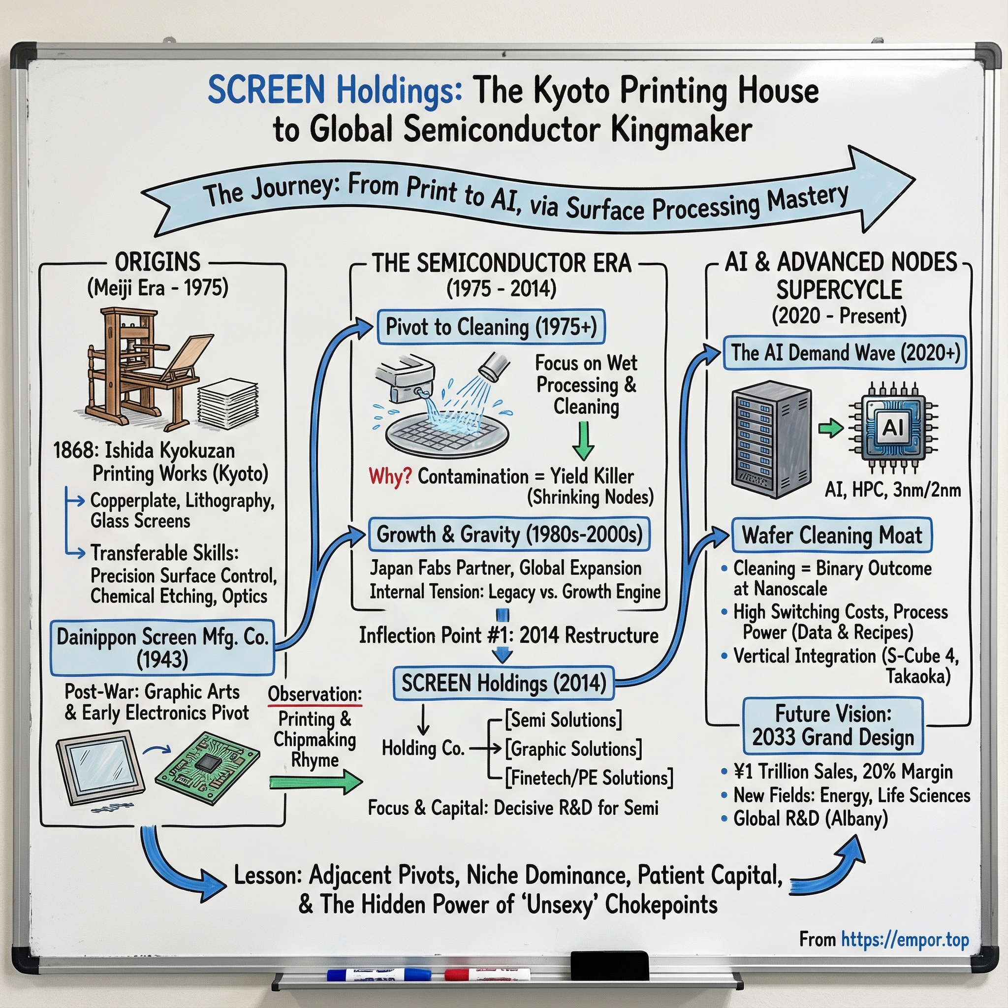
So how does a business go from hand-operated lithographic presses in the age of samurai to mission-critical semiconductor tools in the age of AI? The answer isn’t a single lucky bet. It’s a century-and-a-half pattern of adjacent moves, where the company kept discovering that its real product wasn’t “printing” or “chips”—it was the ability to manipulate surfaces with extreme control.
Today, with a significant market position in non-memory fabs, SCREEN is the top provider of wafer cleaning equipment used in front-end wafer processing in IC fabs. Its systems move through hundreds of wafers per hour, over and over, day after day—helping ensure that the chips inside smartphones, data centers, and AI accelerators can be manufactured at all.
That’s the arc of this story: the power of adjacent pivots, the quiet dominance you can build by owning an unglamorous niche, and Japan’s underappreciated influence over the semiconductor supply chain. Because once you understand SCREEN, you start seeing the industry differently. Steps that sound mundane—like cleaning—turn out to be strategic chokepoints.
And if you’re looking at the semiconductor equipment sector as an investor, SCREEN is a rare combination: century-spanning institutional continuity, paired with direct exposure to the fastest-moving parts of global technology. From Meiji-era Kyoto to the cleanrooms that make AI possible—this is one of the more unlikely, and more instructive, transformations in industrial history.
II. Origins: From Meiji-Era Printing to Glass Screens (1868-1943)
1868 wasn’t just a date on a Japanese timeline. It was a reset. The Tokugawa shogunate fell, the teenage Emperor Meiji took power, and Japan raced to modernize fast enough to avoid becoming a Western colony. Kyoto—ancient, artistic, and suddenly less politically central—was still overflowing with craftspeople who knew how to make difficult things with their hands.
That’s where SCREEN’s story begins. In that same year, in Kyoto, Ishida Kyokuzan founded Ishida Kyokuzan Printing Works, specializing in copperplate and lithographic printing.
Kyoto was the perfect place for it. For a thousand years it had been Japan’s workshop for high craft: woodblock printing, calligraphy, textile dyeing. Those trades weren’t just “art.” They were process disciplines—repeatable, unforgiving, and deeply material. When Western printing techniques arrived during the Meiji era, Kyoto’s artisans had the muscle memory to absorb them.
And lithography, in particular, was sneaky important. It wasn’t just ink on paper. Lithographic printing works because you control how surfaces behave—how certain areas accept oil-based ink while others repel it, how chemical treatments and etching create microscopic patterns that hold detail. It’s surface chemistry, executed with obsessive care. In 1868, nobody was thinking about semiconductors. But the physics didn’t care what decade it was. The same fundamentals would reappear later, at a much smaller scale.
For decades, Ishida Kyokuzan Printing Works built a steady business serving a Japan that was industrializing at full speed—producing books, documents, and reproductions. It survived the turbulence of the late Meiji and Taisho years and kept sharpening its craft.
Then came the first real leap. In 1934, the company succeeded in producing Japan’s first glass screens for photographic reproduction—an achievement that eventually led to the establishment of Dainippon Screen Mfg. Co., Ltd. in 1943.
These glass screens were cutting-edge imaging technology for the era. They enabled high-quality halftone printing by turning photographs into precise dot patterns that presses could reproduce. Making them meant working at the edge of what manufacturing could do: treat glass uniformly, control optical properties, and keep the surface so consistent that tiny defects didn’t ripple into the final image. In other words, it forced the company to level up from “printing” into precision engineering.
It was also the 1930s, and Japan was becoming increasingly isolated and militarized. The ability to produce advanced optical and printing-related equipment domestically wasn’t just commercial—it was strategic. The glass screen success earned recognition from Japan’s industrial establishment, and it pushed the business toward becoming something more formal and scalable.
That formal step arrived during the war. After patents were acquired by Saigiro Ishida and his son Keizo Ishida, Dainippon Screen Manufacturing Company Limited was founded on October 11th, 1943, in Kyoto.
The timing is striking: incorporation in the middle of World War II, when Japanese industry was being mobilized for national priorities. But what mattered wasn’t the moment—it was the capability. Over 75 years, the company had accumulated a technical toolkit: surface chemistry, microscopic precision, optical processing, and the discipline to run complex processes repeatedly without drift. That toolkit would outlive the era that formed it.
Even the name carried ambition. “Dainippon Screen”—“Great Japan Screen”—reflected the nationalism of the time, but also a belief that this wasn’t just a local printing shop anymore. It was an industrial technology company in the making.
For understanding SCREEN today, this origin story is more than trivia. It’s the clearest early signal of the company’s real advantage: not any single product line, but a transferable mastery of surfaces—something that can move from ink and glass to silicon wafers when the world changes underneath you.
III. Post-War Growth & The Pivot to Electronics (1943-1975)
Japan in 1945 was shattered. Cities burned, industry stalled, and the economy was knocked back decades. Kyoto, almost unbelievably, emerged largely untouched—often credited to U.S. Secretary of War Henry Stimson insisting the city’s cultural significance put it off-limits. Whatever the reason, Dainippon Screen came out of the war with something most Japanese manufacturers didn’t: facilities still standing, and a core technical team still intact.
That mattered, because the occupation and the reconstruction era didn’t just rebuild Japan. They rewired it.
Publishing roared back. Businesses needed packaging and advertising. Government agencies needed forms, records, and documents for a new democratic system. In a country rebuilding its institutions and its consumer economy at the same time, the humble act of printing became urgent infrastructure. Dainippon Screen was right there, supplying the pre-press and graphic arts equipment that let Japan communicate, sell, and organize at scale.
By the 1950s and 1960s, the company had built a reputation as one of Japan’s leading printing machinery makers—known for high quality and reliability. It was a proud, defensible position. But it also came with a risk: printing was a mature industry. The next wave of growth wasn’t going to come from faster presses alone.
The next wave was electronics.
Semiconductors, born in American labs, were starting to leak into everything. And Japan’s electronics champions—Sony, Panasonic, Sharp, and others—were climbing rapidly from consumer gadgets toward more sophisticated components, including chips. Inside Dainippon Screen, engineers began to notice something that, in hindsight, looks obvious—but at the time was a strategic epiphany:
Printing and chipmaking rhyme.
Both are fundamentally about putting material onto a surface with extreme control. Both rely on chemistry. Both depend on optics—using light to transfer patterns onto photosensitive layers. In offset printing’s pre-press workflow, you coat a plate, expose it through a mask, and develop the pattern. Swap “printing plate” for “silicon wafer,” and you’ve basically described photolithography—the core patterning step of semiconductor fabrication.
SCREEN would later sum up this long arc simply: since its founding, it kept building tools for printing, while steadily expanding into electronics—semiconductors, displays, and beyond. But in the mid-1970s, that expansion stopped being gradual and started being decisive.
Dainippon Screen introduced its first semiconductor lithography system, applying decades of optical and chemical process know-how to a higher-growth, higher-stakes market. This wasn’t a moonshot. It was an adjacent move into a field that used familiar physics—just with far less tolerance for error.
The timing helped. Japan’s semiconductor industry in the 1970s was on the rise, supported by government industrial policy and the capital spending of major players like Toshiba, Hitachi, NEC, and Fujitsu. New fabs needed equipment. And as circuit dimensions shrank, a new reality set in: contamination wasn’t an annoyance. It was an existential threat. A defect that wouldn’t even register on a printing plate could kill a chip.
That shift pushed Dainippon Screen toward what would become its calling: wet processing, especially cleaning. The company’s semiconductor production equipment business went on to become a leading provider of wafer processing tools globally, particularly in wet etching and cleaning—alongside a broader lineup of systems that support semiconductor manufacturing.
But even in this early phase, the direction of travel was clear. The company began leaning into wafer cleaning equipment: machines designed to strip away contaminants before, during, and after critical process steps. It sounded like a niche. In reality, it was a compounding advantage. As the industry marched from micrometers toward nanometers, cleaning didn’t get easier—it became the gatekeeper for yield, reliability, and ultimately, profitability.
By 1975, Dainippon Screen had evolved into something new: a company with one foot in the dependable world of graphic arts and the other in the volatile, fast-growing world of semiconductors. The printing business brought cash flow and stability. The semiconductor push brought momentum—and a future.
That split identity would power the company for decades. It would also create internal gravity: legacy businesses that wanted investment, and an emerging semiconductor engine that demanded more. Those tensions wouldn’t go away. They would build—slowly at first, then all at once—until SCREEN eventually had to restructure around what it was truly becoming.
IV. Becoming a Semiconductor Equipment Powerhouse (1975-2000)
From 1975 to 2000, semiconductors didn’t just improve. They exploded—from a promising technology into the foundation of the global information economy. The industry loves to tell that story with transistor counts: Intel’s 4004 in 1971 had 2,300 transistors; by 2000, the Pentium 4 had tens of millions. The point isn’t the math. It’s the consequence: every leap in complexity forced an even bigger leap in manufacturing precision.
And that’s where Dainippon Screen found its lane.
The company’s bet on wet processing, especially cleaning, turned out to be one of those “looks boring, ends up essential” decisions. A huge share of fab steps require wafers to be cleaned—before patterning, after etch, after polishing, before deposition—because every major operation leaves behind something you don’t want. Particles. Residue. Trace metals. Films so thin you can’t see them, but thick enough to ruin yield.
To understand why cleaning becomes a chokepoint, you have to understand the paranoia of a modern fab. A logic chip is built from structures measured in nanometers. At that scale, contamination isn’t a quality issue; it’s a binary outcome. One stray particle landing at the wrong moment can become a defect that carries forward through subsequent layers until the chip is dead on arrival.
Wet cleaning sounds simple—spray, rinse, spin, dry—but the chemistry is anything but. Different contaminants need different recipes. The process has to remove what you want gone without attacking what you need to keep. And the cleaning tool itself cannot become the source of new contamination. This is why wet processing vendors win on reliability, repeatability, and know-how that accumulates slowly over decades.
SCREEN leaned hard into that learning curve. Over time, it developed systems like the SS-3200 spin-scrubber, capable of processing hundreds of wafers per hour while reducing deionized-water use—exactly the kind of incremental, engineer-beloved improvement that drives replacement cycles in fabs.
During the 1980s, Dainippon Screen also benefited from something that, in retrospect, looks like the perfect home-market tailwind: Japan’s semiconductor giants. Toshiba, Hitachi, NEC, Fujitsu, Mitsubishi—these companies were scaling aggressively, and for much of the decade Japan led the world in memory production. For SCREEN, that meant a domestic base of demanding customers who funded development, pushed specifications, and—crucially—served as reference accounts when SCREEN went overseas.
The way Japanese industry worked amplified this advantage. Under keiretsu-style norms, equipment suppliers weren’t just vendors. They were collaborators. The expectation was close partnership: co-develop the process, customize the tool, iterate together. That relationship built deep technical knowledge and high switching costs long before “switching costs” became a framework term.
SCREEN institutionalized that collaboration. At its Process Technology Centre (PTC) in Hikone, Japan, it promoted joint development with customers in a substantial cleanroom environment equipped with process and metrology tools—an on-ramp for turning customer roadmaps into SCREEN product roadmaps.
Then the 1990s hit, and Japan’s economic engine stalled. The “Lost Decade” squeezed domestic demand, while Korean competitors—Samsung, Hyundai (later SK Hynix), and LG—invested heavily and began overtaking Japanese companies in DRAM. The center of gravity in memory shifted, and the entire supply chain had to adapt.
Dainippon Screen’s response was to widen its aperture. It expanded its global footprint with sales and service operations across the United States, Europe, Taiwan, and Korea. And it broadened its semiconductor lineup beyond cleaning into adjacent steps like coating, developing, and inspection—staying close to its core competence while becoming more valuable to fabs.
By 2000, the transformation was unmistakable. Dainippon Screen wasn’t a printing company dabbling in semiconductors anymore. It was a global semiconductor equipment supplier that still happened to have a printing business. Its cleaning tools were in fabs across Asia, America, and Europe, supporting everything from PC chips to automotive electronics.
But the success created a new problem: gravity inside the company.
Graphic arts, even if still profitable, was heading into structural decline as digital workflows reshaped printing. Semiconductors, meanwhile, demanded relentless R&D to keep pace with shrinking geometries and rising complexity. Keeping both under one corporate roof meant constant internal trade-offs—capital, talent, attention.
Those tensions didn’t break the company. They set up the next act.
V. Inflection Point #1: The 2014 Holding Company Restructure
By the early 2010s, Dainippon Screen was running into a problem that only success can create. The semiconductor equipment business was surging, lifted by smartphones and the rise of the modern data center. But the company was still organized like a decades-old conglomerate—multiple businesses, all under one roof, all pulling on the same limited pool of capital, engineering talent, and executive attention. The structure that once made diversification easy was now slowing down the one business that needed to move fastest.
On August 5, 2014, the company announced it would change its name from Dainippon Screen Mfg. Co., Ltd. to SCREEN Holdings, and restructure into a holding company.
This wasn’t a paperwork exercise. It was a deliberate reset of how SCREEN would compete. Instead of one operating company trying to manage everything—from bleeding-edge semiconductor tools to mature printing systems—SCREEN moved to a holding-company model with operating subsidiaries designed to run with more autonomy.
Holding company: SCREEN Holdings Co., Ltd. Business operating companies: SCREEN Semiconductor Solutions Co., Ltd. SCREEN Graphic Solutions Co., Ltd. SCREEN Finetech Solutions Co., Ltd. SCREEN PE Solutions Co., Ltd. SCREEN Advanced System Solutions Co., Ltd.
The intent was simple: focus. SCREEN Semiconductor Solutions could now act like what it really was—a frontline semiconductor equipment company—making faster calls on product development, fab support, and customer engagement without waiting for internal consensus across unrelated businesses. Meanwhile, SCREEN Graphic Solutions could run its own playbook in a mature printing market, optimizing for profitability and customer loyalty rather than chasing the cadence of semiconductor cycles. Each unit could build the culture, incentives, and hiring pipelines that matched its reality.
For investors, it also made the story easier to see. The Semiconductor Manufacturing Equipment (SE) segment develops, manufactures, sells, and maintains semiconductor manufacturing equipment. The Graphics and Arts Equipment (GA) segment does the same for printing-related equipment. The Display Manufacturing Equipment and Film Forming Equipment (FT) segment covers display manufacturing equipment and film forming equipment.
And the scoreboard was increasingly clear: semiconductors were the engine. Wafer cleaning and related processing tools accounted for the majority of SCREEN’s revenue and essentially all of its growth, while the graphic arts business—though mature—continued to generate profit and cash.
The rebrand took effect on October 1, 2014, when Dainippon Screen Manufacturing officially became SCREEN Holdings. Even the name was a strategic signal. “Dainippon,” meaning “Great Japan,” carried the imprint of an earlier era. “SCREEN” sounded global—more neutral, more modern, and better aligned with a customer base that now spanned the world’s most important fabs.
Just as important, the new structure made capital allocation more decisive. Instead of watering investment across businesses with very different trajectories, SCREEN could put its money where the future was. In practice, that meant semiconductor equipment: more R&D, more manufacturing capacity, and more ability to support customers at the front edge.
The total investment will be approximately 16 billion yen. Once this new investment package is implemented, SCREEN Holdings expects the total production capacity of its SPE business to increase by around 20%.
The timing couldn’t have been better. The years after 2014 brought another surge in global chip demand—smartphones, cloud computing, and the early momentum of AI. In semiconductor equipment, capacity and readiness compound: the companies that invest ahead of the curve tend to be the ones still standing when the orders flood in.
And the way SCREEN approached it—willing to spend, willing to take some near-term pressure, in exchange for long-term position—fit a distinctly Japanese style of strategy. Less obsessed with optimizing the next quarter, more focused on winning the next decade.
The 2014 restructuring didn’t just tidy up the org chart. It cleared the runway for SCREEN to enter the most important semiconductor cycle yet.
VI. Inflection Point #2: The AI & Advanced Node Supercycle (2020-Present)
After the 2014 restructure, SCREEN had a clearer engine, a cleaner org chart, and a longer runway. Then the industry hit the kind of demand wave that turns “strong positioning” into “strategic gravity.”
Generative AI’s breakout in 2022 and 2023 didn’t just boost chip demand—it reshaped it. Data center operators raced to build GPU clusters for training and inference. Memory makers sprinted to ramp High Bandwidth Memory (HBM). Foundries, led by TSMC, pushed harder into leading-edge nodes. And behind every one of those moves sat the same unglamorous bottleneck: manufacturing yield at absurdly small dimensions.
That’s where SCREEN lives.
In 2024, SCREEN’s revenue rose to 625.27 billion yen, up from 504.92 billion the prior year. Earnings climbed to 99.47 billion yen. In the fiscal year ending March 2025, revenue clearing 625 billion yen and earnings nearing 100 billion yen would have sounded like science fiction not long before—but it fit the new reality: wafer cleaning wasn’t a “nice-to-have” tool category anymore. It was one of the few places where spending tends to increase as chips get harder.
That showed up in the more recent cadence too. SCREEN reported strong second-quarter results in fiscal 2025, with net sales of 274.2 billion yen and operating income of 46.4 billion yen—an operating margin of 16.9%. The point isn’t the quarter. It’s what the quarter represented: demand that’s being pulled forward by structural shifts, not just a typical semiconductor upcycle.
So why does AI translate so directly into wafer cleaning orders?
Because the chips powering AI are the most complex devices humanity manufactures. AI accelerators—like NVIDIA’s Blackwell-class systems or Google’s TPUs—push transistor density and interconnect complexity to the edge of what physics will tolerate. As the industry moves toward 1.6 nm-class process technology, cleaning turns into a survival requirement. At 3nm and 2nm, particles that were once “background noise” become yield killers. Contamination control stops being a quality metric and becomes a binary: the wafer either lives or dies.
And it’s not just about building more fabs. Node transitions force replacement cycles. Even if overall wafer capacity stays flat, the move to tighter specifications demands new cleaning capability, new recipes, and tighter process control. SCREEN gets paid when customers expand, and it gets paid again when customers upgrade.
That dynamic is why the Wafer Front-End market—SCREEN’s core hunting ground—is projected to grow at a mid-single-digit rate in calendar 2026, with AI-related demand as the primary driver.
TSMC is the anchor customer that makes this especially consequential. As the dominant advanced logic foundry, TSMC effectively writes the roadmap everyone else follows. Morgan Stanley has pointed to TSMC’s expected expansion of N3 production capacity by 2026 as a meaningful driver for SCREEN. And the roadmap doesn’t stop at N3. TSMC’s 2nm (N2) technology is slated to begin volume production in 4Q25, featuring first-generation nanosheet transistors and full-node gains in performance and power.
All of that is great for demand—but it doesn’t make the business smooth.
In Q1 of fiscal 2026, SCREEN reported a slight increase in net sales to 135.7 billion yen, up 1.2% year over year, alongside a decrease in operating income. That’s the reality of this phase: SCREEN is investing into the next wave while the market continues to move in uneven bursts. The company described the demand picture in the way you’d expect from an industry being remade in real time: foundries still investing aggressively in cutting-edge nodes on AI pull; logic customers reviewing spend more carefully; memory investing strongly again, led by HBM and DDR demand.
Geography is shifting too, and not subtly. Management has said the proportion of sales from China is expected to decline to around 30%, while still expressing confidence in maintaining profitability. That single line captures two forces pulling at the entire semiconductor equipment sector: export-control pressure from the US-led policy regime, and the steady maturation of China’s domestic equipment ecosystem.
SCREEN is riding the biggest buildout the industry has seen in years—but it’s doing it in a world where the cycle, the node roadmap, and geopolitics are all hitting at once.
VII. The Wafer Cleaning Moat: Why This Niche Matters
To really understand SCREEN’s competitive position, you have to get comfortable with an idea that feels backwards at first: wafer cleaning—way less glamorous than lithography or etch—is one of the most defensible places to build power in semiconductor equipment.
As fabs pushed into advanced nodes below 10nm, the industry’s center of gravity shifted toward single-wafer cleaning. In 2024, single-wafer systems held the largest share of the market for a reason: precision.
Batch cleaning is the old workhorse model. You run multiple wafers together through chemical baths. It’s efficient, and for many use cases it’s perfectly fine—but you’re inherently trading away fine-grained control. Single-wafer tools flip that tradeoff. Each wafer is processed individually, so recipes can be tuned more tightly, wafer-to-wafer uniformity improves, and the risk of cross-contamination drops. As device structures became more complex and tolerances collapsed, “good enough” cleaning stopped being good enough. Even if single-wafer is more expensive on a per-wafer basis, it becomes the only viable approach for the most demanding processes.
And modern cleaning tools aren’t just chemical plumbing. They’re process-control systems—computers wrapped around chemistry and motion.
Machine controllers now log millions of datapoints per lot. The tool tracks and adjusts a long list of parameters—flow rates, temperatures, chemical concentrations, mechanical forces—constantly trying to hold the process steady. On top of that, vendors embed analytics and predictive maintenance that can flag things like nozzle fouling or flow instability before they turn into a line-stopping event.
That software layer creates one of the biggest moats in the category: switching costs. Process engineers learn the quirks and behaviors of a specific platform. Recipes are developed, qualified, and refined on that platform. And moving those recipes—along with the operational confidence they represent—to a competitor isn’t just a procurement decision. It’s a risk decision.
Competition, of course, doesn’t stand still. Tokyo Electron’s cryogenic etch has been highlighted for cutting CO₂ emissions by 80%, and ACM Research’s Ultra C Tahoe reduced sulfuric-acid use by 75% while matching legacy performance—enough to win multiple foundry installs. The direction is clear: environmental performance is becoming part of the spec.
That matters because semiconductor fabrication consumes staggering volumes of ultra-pure water and produces hazardous chemical waste. Regulators are paying closer attention. Customers are, too. Equipment that can hit performance targets while reducing water and chemical consumption isn’t just “nice.” It’s becoming a requirement. SCREEN’s emphasis on water-efficient designs and reduced chemical consumption fits directly into that shift.
Of course, having the best product on paper is only half the game. The other half is building enough of them, fast enough, when the cycle demands it.
In January 2023, SCREEN Holdings completed construction of its new factory, S-Cube 4, dedicated to semiconductor production equipment. It was built at the existing Hikone Site, a meaningful expansion of SCREEN’s manufacturing footprint. More broadly, the company’s recent investment program—S-Cube 3, S-Cube 4, S-Cube 5, and the Takaoka plant—has been aimed at expanding production capacity so SCREEN can meet demand surges without punishing lead times. SCREEN anticipates the construction of the new S3 (S-Cube) facility will expand its present manufacturing capacity by around 150%.
The Takaoka Plant shows how seriously SCREEN takes operational control. SCREEN opened it in Takaoka City, Toyama Prefecture, to bolster production capacity for its Semiconductor Production Equipment (SPE) business. It’s dedicated to producing chemical solution cabinets for SCREEN’s single-wafer cleaning systems—flagship products for the segment. The plant is set up to complete everything from assembly to inspection non-stop, improving productivity and efficiency across the SPE business.
That’s also vertical integration in action. By producing chemical cabinets in-house instead of relying on third parties, SCREEN reduces supply-chain vulnerability and keeps proprietary process knowledge closer to home—an increasingly valuable advantage in an era where disruptions aren’t rare outliers, they’re part of the operating environment.
The investor takeaway is simple: wafer cleaning is not a commodity business. The technical complexity, multi-year qualification cycles, deep customer relationships, data-driven process lock-in, and the gravity of the installed base create real barriers to entry. SCREEN’s leadership here isn’t the result of a single breakthrough—it’s the compound interest of decades of cumulative investment, and that’s the kind of advantage competitors can’t quickly copy.
VIII. The Multi-Business Portfolio: Legacy & Opportunity
By now, SCREEN can look like a pure-play semiconductor equipment story. In practice, it’s still a portfolio—one shaped by history, but also by a very intentional strategy: keep the semiconductor engine dominant, while continuing to place smaller bets in adjacent “surface processing” arenas.
SCREEN Holdings operates four major business divisions, each with its own rhythm and end market. Semiconductor production equipment is the center of gravity. Around it sit businesses with very different demand cycles and very different definitions of “innovation”: graphic arts systems for printing, flat panel display manufacturing equipment, and printed circuit board-related equipment.
SCREEN describes the arc plainly: since its founding, it has continued to develop tools for the printing industry while expanding into electronics—semiconductors, displays, and other fields. More recently, it has widened the scope again to include advanced semiconductor packaging, energy, and life sciences, aiming to offer a broader range of solutions without abandoning the technical spine that made those expansions possible.
The most direct legacy business is graphic arts—essentially the company’s origin story, industrialized. SCREEN manufactures printing equipment for a wide range of markets: books, labels, folding cartons, newspapers, direct mail, transpromo, packaging, wide-format, and commercial printing. This is not a market with the same growth curve as semiconductors. Traditional printing has been in secular decline for years. But it isn’t simply “dying” either. Digital inkjet has created real pockets of growth, especially where speed, customization, and shorter runs matter—packaging, labels, and specialty applications where print is still a product feature, not just a distribution method.
Then there’s the forward-looking part of the portfolio: energy. SCREEN has said it plans to expand space for producing hydrogen-related equipment and components, including cell stacks for water electrolysis and membrane electrode assemblies (MEA) for fuel cells—areas where it expects future growth. Alongside that, it will establish a new administrative office in the same building to accommodate headcount growth in its semiconductor production equipment (SPE) business, a small but telling reminder of where the demand pressure is most acute.
The energy push is the more speculative bet, but it isn’t random. SCREEN’s playbook has always been to reuse core know-how in new contexts, and coating and surface treatment map naturally onto manufacturing challenges in fuel cells and electrolyzers. MEAs, in particular, demand controlled, repeatable deposition on sensitive materials. Whether this business reaches real scale is still an open question—but as a strategic move, it fits the company’s pattern: look for industries where “how you treat the surface” is the difference between working and not working.
All of this ladders up to the company’s longer-term ambition. SCREEN’s 10-year Management Grand Design sets a high bar: over 1 trillion yen in net sales, while expanding into emerging industries like energy and life sciences.
The unifying idea—the thing that keeps this from feeling like unrelated diversification—is the “Surface Processing” thesis. Whether the substrate is paper, silicon, glass, or polymer membranes, SCREEN keeps coming back to the same underlying skill: controlling materials at interfaces with extreme precision. That commonality may matter more in engineering meetings than in investor decks, but it helps explain why these expansions aren’t starting from zero.
For investors, this portfolio cuts both ways. The semiconductor business drives growth and earns the premium narrative. The other segments are smaller and more modest, but they can provide ballast when the semiconductor cycle inevitably turns. The hard part—and the real management test—is capital allocation: deciding how much to reinvest into the semiconductor engine, how much to defend and harvest mature businesses like graphics, and how much to place into newer bets without losing focus on the core.
IX. Strategic Vision: The 2033 Grand Design
If the 2014 restructure cleared the runway, the company’s 2033 plan is SCREEN telling the market exactly where it intends to land.
SCREEN’s long-term planning reflects a distinctly Japanese approach to corporate strategy: think in decades, not quarters; set a direction big enough that it shapes decisions across cycles.
We will also invest proactively for future growth to achieve our 10-year goals – net sales of ¥1 trillion or more and operating margin of 20% or above – in the fiscal year ending March 31, 2033, as set out in the Management Grand Design announced in September 2023.
Those targets are deliberately ambitious. The trillion-yen revenue goal implies major growth from today’s scale, and the 20% operating margin implies the company believes it can get not just bigger, but structurally more profitable as it scales.
SCREEN framed the nearer-term path as an intentional build phase:
The three years covered by Value Up Further 2026 will be an investment phase, building a momentum for new growth while maintaining the financial foundation established in the past four years, for achieving the ¥1 trillion net sales target 10 years later.
In other words: expect spending before you see the full payoff. Management has been clear that near-term margins may compress as it invests in capacity, R&D, and new business development. That tradeoff—less optimization now, more competitive position later—is a pattern you see in Japanese industrial champions when they’re serious about a category.
A big chunk of that investment is physical. SCREEN plans significant capital spending to strengthen its production and service systems for semiconductor production equipment (SPE), with a goal of lifting total production capacity by about 20%.
Capacity keeps showing up because lead times in semiconductor equipment are brutal. A tool ordered today might not ship for years. If you wait until the cycle is hot to expand, you’re already too late. SCREEN’s stance is basically: invest through the cycle so you’re ready when the orders hit.
But the Grand Design isn’t only about building more tools in Japan. It’s also about putting SCREEN’s process know-how where the next wave of semiconductor development is happening.
Under the agreement, SCREEN will invest more than $75 million during the first three years of a broader 10-year partnership. The company will use 10,000 square feet of cleanroom space in NY Creates' new NanoFab Reflection building and 5,000 square feet of office space at the Albany site.
This Albany R&D center is one of SCREEN’s most meaningful commitments outside Japan. Governor Kathy Hochul today announced a strategic international partnership between NY Creates and SCREEN, a Japan-based semiconductor equipment manufacturing company and leader in wet etching and cleaning applications. SCREEN President and CEO Masato Goto said, "SCREEN appreciates the cooperation of NY Creates and Empire State Development parties to enable us to establish our new R&D site outside Japan at the Albany NanoTech Complex with the aim of reinforcing our product competitiveness in the semiconductor production equipment business."
Strategically, it does a few things at once. It puts SCREEN closer to U.S. customers expanding domestic fabrication under CHIPS Act incentives. It plugs the company into Albany’s collaborative research infrastructure. And it signals commitment to the U.S. market at a time when geopolitics increasingly influences which tools fabs want to qualify—and which suppliers they want to build long-term process roadmaps with.
X. Porter's Five Forces Analysis
To make sense of SCREEN’s position, it helps to step back from the product details and look at the industry through a simple lens: what forces decide who earns great returns, and who gets ground down?
Threat of New Entrants: LOW
On paper, wafer cleaning might sound like a category a smart team could “just build.” In reality, it’s a minefield of barriers that only look invisible because the incumbents have already cleared them.
The biggest gate is qualification. Before a cleaning tool ever touches high-volume production, it has to survive extended, on-site testing at the customer. That process typically takes 2–4 years. It’s expensive, slow, and brutal: the vendor has to prove not only performance, but repeatability, uptime, and the ability to support the tool in the messy realities of a fab. A new entrant has to fund years of development and field work before meaningful revenue shows up—while the established players keep selling to their installed base.
That installed base becomes its own fortress. Process engineers build deep familiarity with a platform. Recipes get tuned and retuned over years until they’re not just “settings,” they’re institutional knowledge. So when a fab considers replacing equipment, the switching cost isn’t the price of the tool. It’s requalification risk, recipe redevelopment, and retraining—plus the uncomfortable fact that a mistake here can kill yield.
Bargaining Power of Suppliers: MODERATE
A wafer cleaning system is an orchestration of specialized inputs: precision robotics, ultra-pure chemical delivery, advanced sensors, control electronics. Some components have limited supplier options, which creates real leverage and potential bottlenecks.
But SCREEN has been intentionally taking some of that leverage back through vertical integration. The Takaoka Plant, for example, is dedicated to producing chemical solution cabinets for SCREEN’s single-wafer cleaning systems—its SPE flagship products—and is designed to run the full flow from assembly to inspection continuously. Moves like that don’t eliminate supplier risk, but they reduce dependency in areas that can become painful during demand surges or disruptions.
Bargaining Power of Buyers: MODERATE-HIGH
SCREEN’s customers are some of the most sophisticated buyers in the world. TSMC, Samsung, Intel, and the major memory manufacturers spend enormous amounts on equipment, and they have the technical depth to evaluate competing tools with a level of rigor most industries never see. They can push hard on terms, support commitments, and roadmap alignment.
But here’s the counterweight: this is not an equipment category where “close enough” is acceptable. If a cleaning system misses contamination specs, it doesn’t just underperform—it can destroy massive value in in-process wafers. That reality limits how aggressively buyers can treat cleaning as a bargaining chip. Reliability and process capability matter more than small price differences, and switching vendors introduces risk that even the largest fabs are reluctant to take lightly.
Threat of Substitutes: LOW
Big industry shifts—EUV adoption, new foundry build-outs across Taiwan, South Korea, China, and the United States, and transitions to new wafer types like silicon-carbide and gallium-nitride—are expanding the universe of wafers that need to be processed and cleaned.
And despite ongoing innovation, wet cleaning remains the default for most applications. Dry cleaning methods exist, but they tend to live in specialized niches rather than replacing wet chemistry broadly. For the majority of contamination types and sizes, liquid-based approaches still win on the underlying physics of removal.
Industry Rivalry: MODERATE-HIGH
This is a concentrated arena with heavyweight competitors: SCREEN Holdings, Tokyo Electron, Applied Materials, Lam Research, and Shibaura Mechatronics, among others. Rivalry is intense—but it’s usually fought on technology and performance, not on price. In fact, competing primarily on cost can backfire, because customers tend to distrust bargain positioning for equipment that sits at the heart of yield.
The most notable competitive wrinkle in recent years has been ACM Research. It’s captured share through localized supply chains in China and product wins like Ultra C Tahoe. That focus—serving Chinese customers amid export-control uncertainty—has helped create a credible challenger the incumbents can’t ignore, especially in a region where the center of gravity is increasingly strategic, not just commercial.
XI. Hamilton's 7 Powers Framework Analysis
Porter tells you what the battlefield looks like. Hamilton Helmer’s 7 Powers tries to answer a different question: if two companies are standing on the same battlefield, why does one keep winning year after year?
1. Scale Economies: MODERATE
In semiconductor equipment, scale doesn’t work the way it does in consumer electronics. This is a precision business first, and a volume business second. If you have the better process capability, you can win accounts even if you’re smaller.
But scale still matters in one crucial place: R&D. Next-generation cleaning tools demand deep investment in process engineering, materials science, and increasingly software. SCREEN’s leadership position lets it spread those costs across a broader customer and revenue base than smaller competitors can.
2. Network Effects: LOW
Classic network effects don’t really apply here. A cleaning tool doesn’t become more valuable just because more fabs buy it.
That said, there are ecosystem effects at the edges. Widely adopted platforms can benefit from an expanding pool of engineers trained on the tool, and a growing library of process know-how and recipes that circulate through the industry. It’s not a true network effect, but it does create a subtle “default choice” momentum over time.
3. Counter-Positioning: MODERATE-HIGH (Historically)
SCREEN’s move from printing into semiconductors is almost textbook counter-positioning. Other graphic arts competitors could have attempted the same pivot, but doing so would have forced them to disrupt their own business models and cultures—shifting away from known markets, known customers, and known product cycles, with no guarantee the semiconductor bet would pay off.
Today, that dynamic shows up differently. SCREEN is no longer the upstart. Instead, newer players—especially Chinese competitors like ACM Research—have counter-positioned against incumbents by tailoring products and operations to the specific needs and constraints of the Chinese market.
4. Switching Costs: VERY HIGH
If SCREEN has one power that consistently shows up in practice, it’s switching costs.
Once a cleaning process is qualified for production—a validation that can take months of testing and consumes huge numbers of wafers—switching vendors becomes a high-stakes gamble. Recipes built on SCREEN tools aren’t generic settings you can copy-paste. They reflect years of optimization that’s specific to the equipment’s behavior, and they live inside the habits and instincts of the engineers running the line.
Even when a competitor claims better specs, fabs have to weigh a hard truth: the cost of being wrong is measured in yield loss, not in purchase price.
5. Branding: MODERATE
SCREEN isn’t a consumer brand, but inside semiconductor fabs it has real brand weight. Engineers know it for reliability, and that reputation matters in a category where “mostly works” is not acceptable.
The company frames this identity through its corporate purpose, “Innovation for a Sustainable World,” and its long-term vision, “Be a Solution Creator.” Whatever you think of slogans, the underlying point is practical: SCREEN has built trust with the people who sign off on process tools.
6. Cornered Resource: MODERATE-HIGH
Some assets are hard to buy and even harder to copy. SCREEN has a deep reservoir of tacit know-how built from more than a century and a half of surface processing—knowledge about materials, chemistry, and equipment design that doesn’t fully translate into patents or manuals.
Then there are relationships. Decades of collaboration with leading fabs give SCREEN early visibility into customer roadmaps and emerging requirements. New entrants can offer discounts. They can’t instantly recreate that depth of access and shared process history.
7. Process Power: HIGH
SCREEN’s most durable advantage may be process power: the compounding benefit of repeated learning across thousands of installs.
Every tool in the field generates feedback—what fails, what drifts, what improves yield, what’s harder to service than expected. That learning gets folded into the next design, which makes the next tool better, which produces more learning. It’s a loop.
And it’s accelerating because the tools themselves are getting smarter. Cleaning systems now capture enormous streams of telemetry; machine controllers can store millions of datapoints per lot. Predictive maintenance can flag issues like nozzle fouling or flow instability before they trigger downtime. The more instrumented the equipment becomes, the more valuable the installed base becomes—because it generates more operational data to refine the next generation.
In that world, leadership isn’t just a market share statistic. It’s an information advantage.
XII. Competitive Landscape & Positioning
SCREEN plays in a market where the map is simple: a small number of companies take most of the wafer cleaning revenue, and the fights are decided by process capability, trust, and qualification history—not by who can shave a few points off the price. To understand SCREEN’s room to maneuver, you have to look at the other heavyweights in the ring.
Tokyo Electron (TEL): TEL is Japan’s largest semiconductor equipment company, and unlike SCREEN it’s broadly diversified—deposition, etch, cleaning, coating, and more. In practice, TEL and SCREEN live inside the same Japanese industrial ecosystem: close to the same customers, often in the same fabs, sometimes competing head-to-head and sometimes simply solving different parts of the same problem. TEL’s breadth gives it resilience and cross-selling power. SCREEN’s narrower focus lets it go deeper in cleaning, where “good” isn’t good enough.
Applied Materials and Lam Research: These U.S. giants are best known for other battlefield positions—Applied in deposition, Lam in etch—with cleaning sitting as a smaller part of much larger portfolios. Their edge is systems integration: they can sell customers a more comprehensive process solution rather than a single category tool. SCREEN’s counter is specialization. When customers break decisions apart and demand best-in-class cleaning performance, specialists can win—especially in a process step where tiny deltas show up as yield.
That competitive posture also shows up in how SCREEN returns capital. SCREEN’s dividend policy targets a consolidated payout ratio of 30% or above. That looks different from many U.S. peers, who often lean more heavily on share buybacks. Relative to TEL—often discussed as targeting around a 50% payout—SCREEN’s approach is more conservative. But it can still translate into a higher direct dividend return than Applied Materials or Lam Research.
ACM Research: The most important competitive shift in recent years has come from ACM, which has built a meaningful position in China. ACM Research grew 40% to USD 782.1 million by expanding installs at Chinese foundries, particularly at 28 nm and below. Export controls matter here: when restrictions limit SCREEN and other established players from serving certain Chinese customers, ACM can step into the gap and compound share in a market that’s working hard to localize its supply chain.
SEMES: SEMES is a different species of competitor. It’s Samsung’s captive equipment subsidiary—vertical integration by one of the world’s most important buyers. SEMES primarily serves Samsung’s own fabs, which caps its open-market impact, but it still represents a formidable model: a “competitor” with guaranteed demand and direct access to leading-edge requirements.
Zoom out, and the competitive landscape is inseparable from Japan’s role in the global equipment supply chain. Japan is one of the world’s key semiconductor equipment hubs, with champions like Tokyo Electron and SCREEN. Notably, Japan was China’s largest source of semiconductor manufacturing equipment in 2022, accounting for about a third of China’s imports in the category.
That brings us to the force that now sits over every strategy discussion: geopolitics. Japan’s alignment with U.S. export-control policy has tightened access to parts of the Chinese market. In 2023, Japan expanded export restrictions covering 23 types of cutting-edge semiconductor manufacturing technologies, following U.S. actions restricting China’s access to crucial fabrication tools.
SCREEN’s response is pragmatic: lean into mature-process equipment that isn’t subject to export controls where possible, and keep expanding alternatives—customers and capacity—in the U.S., Europe, and allied Asian countries. In a world where the market is big but not fully accessible, positioning isn’t just about product anymore. It’s about where you’re allowed to sell, where you can support long-term roadmaps, and how you keep your growth engine running when the rules change mid-cycle.
XIII. Bear vs. Bull Case
Bull Case:
The case for SCREEN starts with a simple idea: the harder chips get to make, the more valuable cleaning becomes.
As geometries shrink toward the industry’s 1.6 nm direction of travel, contamination specs tighten to the point where removing sub-10 nm particles isn’t an optimization—it’s mandatory. And that doesn’t just benefit new fabs. Every node transition raises the bar inside existing fabs too, which pulls cleaning tools into upgrade cycles even when total wafer capacity isn’t exploding.
The second tailwind is that AI demand looks more like infrastructure than gadgets. SCREEN’s core hunting ground, the Wafer Front-End market, is projected to grow at a mid-single-digit pace in calendar year 2026, with AI-related demand as the key driver. And unlike consumer electronics, where demand can whipsaw with sentiment, AI buildouts are driven by hyperscalers and enterprises allocating capital for data centers—demand that can be lumpy, but often less tied to consumer moods.
Third, advanced packaging is opening new surface problems to solve. High Bandwidth Memory, chiplets, and 2.5D/3D integration all introduce bonding steps where “good enough” surfaces aren’t good enough anymore. Cleaning requirements expand beyond traditional front-end manufacturing because bonding, stacking, and interconnect formation are unforgiving. The expectation that OSAT growth will outpace the broader market reflects that packaging is becoming a bigger share of where performance is won—and where defects are created.
Finally, governments are now subsidizing the very thing SCREEN sells into: more domestic manufacturing capacity. The U.S. CHIPS Act, Japan’s semiconductor revival efforts, and Europe’s sovereignty push are all designed to accelerate fab construction and upgrades. Those facilities still need the same core toolsets—and cleaning is one of the least optional categories in the fab.
Bear Case:
The bear case begins with the truth that never goes away in semiconductor equipment: it’s cyclical.
Even if the long-term trend is up, spending swings with the capex plans of a small number of giant customers. If chip demand weakens and fabs pull back, equipment orders fall fast. On top of that, currency volatility can move reported results around, and competition in wafer cleaning remains intense.
Then there’s China. Export controls and regulatory changes can reduce what SCREEN is allowed to sell and where it can sell it, shrinking the addressable market. That doesn’t just remove revenue—it creates openings. Chinese suppliers like ACM Research can benefit from restrictions that limit foreign incumbents, gaining installs and experience that could translate into stronger global competition over time.
Technology disruption is the other long-tail risk. Wet cleaning dominates today, but alternative approaches—cryogenic cleaning, plasma-based methods, or novel chemistries—could shift where the advantage sits, and toward companies with different strengths.
And hovering over everything is geopolitics. U.S.-China technology competition puts Japanese equipment makers in a difficult spot: many of their customers and growth opportunities are in Asia, while many of the rules and alliances that govern advanced-node tools are shaped by the United States. Export controls implemented across 2023 and 2024 tightened constraints on sales of advanced chipmaking equipment to China.
In other words, SCREEN isn’t just navigating a cycle. It’s navigating a cycle while the map is changing. If tensions escalate and suppliers are forced into sharper choices between markets and alliances, Japanese companies could find themselves caught in the middle—and that could become a structural headwind, not just a temporary one.
XIV. Key Performance Indicators & Investor Lessons
If you’re following SCREEN as an investor, it helps to keep your eye on a few signals that cut through the noise of any single quarter.
1. Semiconductor Equipment Order Backlog
In semiconductor equipment, orders are often the cleanest window into the future. Revenue is lagging; orders are leading.
Watch the book-to-bill ratio—new orders received versus equipment shipped. When it’s consistently above 1.0, backlog is building and demand is outrunning supply. When it’s below 1.0, the industry is usually cooling, and deceleration tends to show up in reported sales later.
2. Operating Margin Trajectory
SCREEN has laid down a clear marker: a 20% operating margin target by fiscal 2033. The day-to-day question is whether the company is moving toward that outcome, or away from it.
Margin expansion in a growing market can be a sign of pricing power and operational leverage—proof that SCREEN is not just riding the cycle, but strengthening its position inside it. Margin compression can mean the opposite: input costs rising faster than price, competitors getting more aggressive, or the company spending heavily ahead of demand.
3. Geographic Revenue Mix
Where SCREEN sells matters almost as much as what it sells.
The mix across Taiwan, Korea, China, Japan, the U.S., and Europe is a real-time read on both customer concentration and geopolitical exposure. Diversification reduces the risk of any one region dictating the company’s fate. Rapid shifts in mix can also tell you something strategic is happening—either a change in market access, a change in customer investment patterns, or a change in competitive dynamics.
Lessons for Investors:
The SCREEN story isn’t just interesting because it’s improbable. It’s useful because it’s repeatable in principle.
The power of adjacent pivots: SCREEN didn’t “start over” when it moved beyond printing. It carried forward transferable capabilities—surface chemistry, optics, precision process control—and applied them where the value was compounding faster. The investor lesson is to look for companies whose true advantage is a capability, not a product.
Niche dominance over broad mediocrity: SCREEN didn’t try to be everything in semiconductor equipment. It went deep in wafer cleaning and wet processing, and built leadership where reliability, recipes, and qualification history create real barriers. In complex industries, depth in one critical step can beat breadth across many.
Patient capital enables transformation: This was a multi-decade evolution, with long stretches where the payoff wasn’t obvious. SCREEN’s ability to keep investing—through cycles, through shifts in end markets, through internal restructuring—is a reminder that the best industrial compounding often requires timelines that don’t fit a short-term mindset.
Hidden power in unsexy niches: Wafer cleaning will never be as flashy as lithography or AI accelerators. But it’s a chokepoint, and chokepoints capture outsized value. The enabling infrastructure behind headline technologies is often where the most durable economics live.
One more investor-relevant piece of the story is capital returns. SCREEN maintains a clear dividend policy, aiming for consistency while still reinvesting aggressively in capacity and R&D. In a cyclical industry, that balance matters: it signals confidence in the durability of the business, without pretending the cycle doesn’t exist.
And ultimately, that’s what SCREEN’s history keeps teaching. Corporate longevity isn’t about defending the first thing you were good at. It’s about recognizing what you’re actually good at—and having the discipline to reapply it as the world changes.
As semiconductor manufacturing pushes toward atomic-scale precision, it’s almost poetic: the surface-processing expertise that started with lithographic work in Kyoto is more relevant than ever. The particles SCREEN removes today are measured in nanometers. The know-how that makes that possible has been compounding for more than 150 years.
 RSS Feed
 Spotify
 Apple Podcasts
 Amazon Music
 Audible
 YouTube