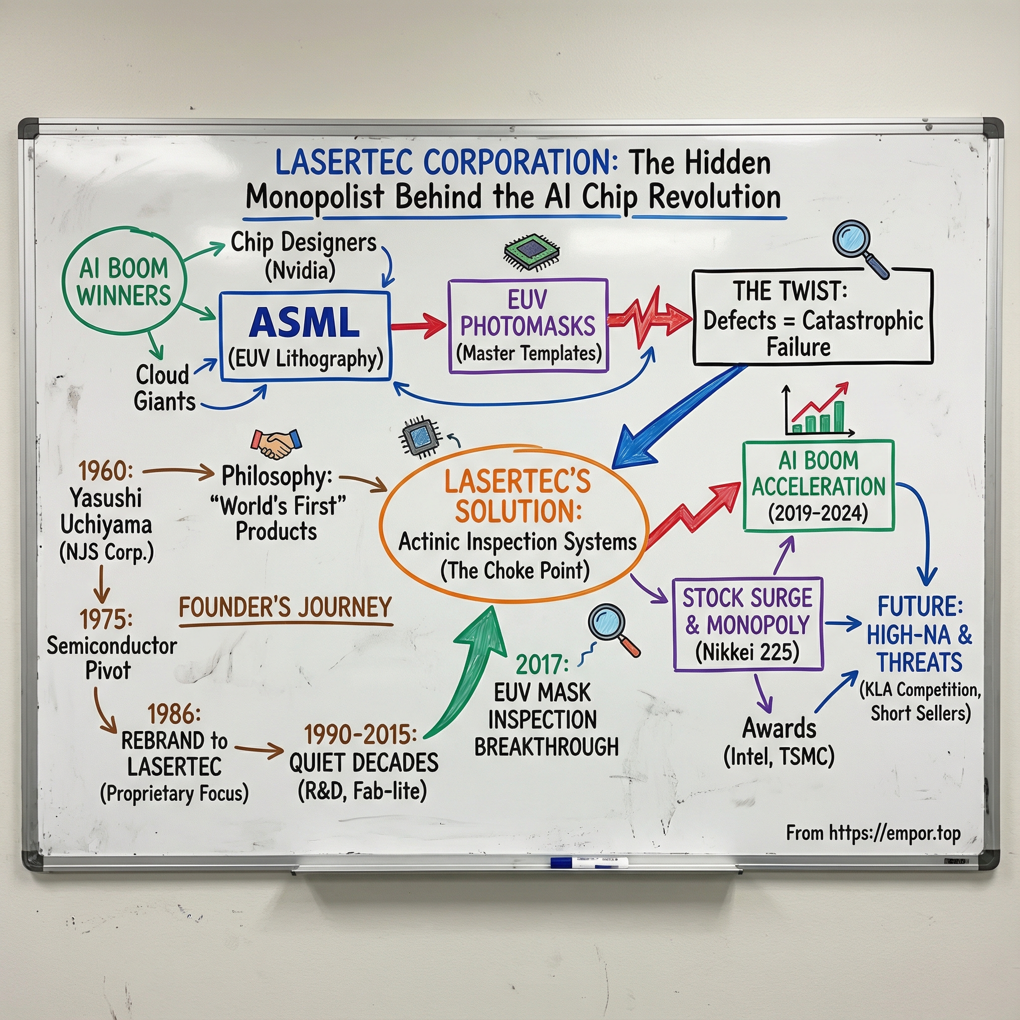
Lasertec Corporation: The Hidden Monopolist Behind the AI Chip Revolution
I. Introduction and Episode Roadmap
In the summer of 2024, something strange happened in the usually buttoned-up world of Japanese equities. Lasertec Corporation, a company most investors couldn’t have picked out of a lineup five years earlier, became the most actively traded stock on the Tokyo Stock Exchange. Its shares had climbed almost 1,800% since 2019, a run so dramatic it helped earn Lasertec a spot in the Nikkei 225 in 2023.
So what is this company, and why did the AI boom suddenly make it unavoidable?
Because Lasertec sits at a choke point in the most advanced manufacturing process on Earth.
To understand how, you have to start with extreme ultraviolet lithography, or EUV, the crown jewel of modern chipmaking. EUV is how you print the tiny features that power today’s leading-edge chips. And as of 2025, there’s only one company that can deliver EUV lithography systems at scale: the Dutch giant ASML. These machines take years to build and cost hundreds of millions of dollars each.
But here’s the twist: even the world’s most important machine is useless without the masks that feed it.
Photomasks are the master templates that project circuit patterns onto silicon wafers. In EUV, those masks are extraordinarily complex, and they have to be nearly perfect. A defect that’s invisible or dismissed in older lithography can become catastrophic at EUV—silently wrecking yields, performance, and entire production runs.
That’s where Lasertec comes in.
Lasertec makes the inspection systems that determine whether EUV masks and mask blanks are good enough to use. In this niche, the company has been the first to commercialize critical tools, including an EUV mask blank inspection system it began selling in 2017. And today, Lasertec holds effectively all of the market for EUV mask blank inspection tools and EUV mask inspection tools, used both in mask shops and inside wafer fabs.
This episode is the story of how that happened: a founder with an obsession for building things no one had built before; a company that kept funding optics-heavy R&D through decades when Japan’s economy stagnated; and a strategy built around chasing “world’s first” products until it landed on the narrow bridge everyone has to cross to make advanced chips.
And then, once you’re the bridge, the next question becomes inevitable: what happens when someone finally tries to build a second one?
II. The Founder's Vision: Yasushi Uchiyama and the Birth of Innovation (1960-1975)
It’s 1960. Japan is in the middle of its postwar economic miracle, rebuilding its identity around technology, precision manufacturing, and a relentless pursuit of quality. In Yokohama, a young engineer named Yasushi Uchiyama makes a choice that, in hindsight, sets the first domino in a chain that leads all the way to today’s AI chip boom.
Uchiyama had a solid job at a major electronics manufacturer. But he wasn’t wired for incremental improvements inside a big organization. He wanted to build products of his own, especially the kind that didn’t exist yet. Not “better.” New.
So in July 1960, he founded Tokyo ITV Laboratory. Two years later, in 1962, the business was incorporated as NJS Corporation, putting a formal structure around what was essentially Uchiyama’s personal mission: make novel technology, and keep making it.
The early work wasn’t glamorous, but it was exactly the kind of technical training ground that would define the company. NJS operated as a subcontractor for Matsushita Communication Industrial Co., Ltd., designing and developing X-ray TV cameras for medical use. This was applied optics under real-world constraints—high precision, high reliability, and no room for hand-waving. It didn’t look like semiconductors yet, but it built the muscle.
Around this time, the company moved from being a workshop-with-a-client to something more independent. The original Tokyo ITV name gave way to NJS—Nihon Jido Seigyo, or Japan Automatic Control—signaling a broader ambition than one contract.
And then Uchiyama laid down the rule that would shape everything that followed: every year, develop and release an innovative product. Not as a nice-to-have. As the company’s operating system. It’s the kind of principle that sounds like a slogan until you realize what it forces culturally: constant R&D, constant risk-taking, and a deep belief that “world’s first” isn’t a headline—it’s the point.
By 1971, NJS released its first original-brand product. That mattered because it marked the moment the company stepped beyond subcontracting and into the harder game: betting its future on technology it owned, sold, and had to stand behind.
This is the throughline investors often miss when they look at Lasertec’s modern dominance and try to reverse-engineer it as a clever strategy. It wasn’t a late-stage pivot or a spree of acquisitions. It was the compounding effect of a founder’s obsession—turned into a culture—built through years of solving brutally precise optical problems and insisting, year after year, on making something nobody else had made.
III. The Semiconductor Pivot: From Medical Equipment to Chip Manufacturing (1975-1985)
By the mid-1970s, NJS had built real confidence in applied optics. The question was where to point it next. And the answer happened to be the fastest-growing, most unforgiving manufacturing industry on the planet: semiconductors.
This was the era when chipmaking was scaling up and getting complicated fast. Intel’s first microprocessor had kicked off a new kind of arms race. Japan’s electronics giants were ramping. And as feature sizes shrank, the same enemy kept showing up everywhere: defects.
In chip manufacturing, photomasks are the master templates. They’re the stencils that carry a circuit pattern and project it onto silicon wafers through photolithography. If the mask is wrong, everything downstream is wrong—repeated hundreds or thousands of times. A tiny defect doesn’t just create a tiny problem. It can quietly destroy yields, schedules, and profits.
NJS saw that inspection was becoming the choke point. So the company moved from medical X-ray imaging into photolithography inspection systems, and in 1975 launched its first semiconductor-market product: an LSI photomask pinhole inspection system—another “world’s first.”
A year later came the product that truly set the trajectory. In 1976, the company developed the world’s first LSI photomask inspection system. The impact wasn’t subtle: it helped customers dramatically reduce costs and gave NJS a platform it could build on for decades.
Because up to that point, a lot of photomask inspection was painfully manual—skilled technicians staring through microscopes, hunting for flaws that were easy to miss and hard to reproduce consistently. Automation changed the game. It made inspection faster, more uniform, and more scalable. In other words, it turned a fragile human step into a manufacturing process.
And in semiconductor equipment, that matters even more than having a clever product. Once a factory qualifies a tool and builds it into the flow, the tool becomes “the way we do things here.” Switching later is slow, expensive, and risky. By being early, NJS wasn’t just selling machines. It was embedding itself into how chips got made.
The company kept pressing its advantage in inspection and optics. It developed a confocal color laser microscope using its optical technology and went on to introduce products like an LCD photomask inspection system and a semiconductor mask blank inspection system—tools that became de facto standards in their niches.
NJS was also starting to look outward. In 1979 it opened a branch in San Mateo, and in 1980 another in Düsseldorf. These were more than sales offices. They were front-row seats to the world’s most demanding chipmakers—and a way to stay close to the next set of problems worth solving.
By the mid-1980s, the pattern was emerging. Find a critical inspection bottleneck. Build something no one else has. Become the tool customers qualify around. Then keep improving it until it’s not just preferred, but difficult to replace.
It was a strategy built for patience. And it would eventually pay off in a way almost no one could have predicted—when lithography itself took a physics-defying leap, and inspection became even more essential than printing.
IV. The Strategic Rebrand: From NJS to Lasertec (1986)
Corporate rebranding is usually marketing theater—a new logo, a new tagline, the same business underneath. In 1986, this wasn’t theater. It was a line in the sand.
That year, NJS renamed itself Lasertec Corporation, right as it delivered another “world’s first”: a color laser scanning microscope. The timing wasn’t accidental. The microscope, known as the 2LM11, was proof that the company’s real asset wasn’t any single product line. It was a core capability: applied optical technology, pushed to the edge of what was possible.
And Lasertec wanted the world—and its own employees—to understand that this was the point.
The new name signaled an intent to pursue opportunities beyond semiconductors, but the more radical move was internal. Lasertec ended its subcontract business entirely. From that moment on, original-brand products would make up 100% of sales. No more dependable work building to someone else’s spec. No more quiet revenue stream to smooth out the risk. The company would live or die on the strength of what it could invent, build, and sell under its own name.
For a Japanese company in the 1980s, that was a real leap. Japan’s industrial system prized stability—long-term supplier relationships and predictable roles in a larger ecosystem. Lasertec walked away from that security because subcontracting came with a ceiling. If you’re always executing someone else’s roadmap, you don’t develop your own. You don’t build the proprietary know-how that turns into pricing power and long-term leverage.
In other words: if you wanted to be indispensable, you couldn’t stay interchangeable.
Even the name was unusually blunt: “Laser” plus “technology.” It wasn’t trying to sound bigger than it was. It was telling you exactly how it planned to compete—not on cost or scale, but on precision optics, on technical leadership, and on being first.
Around the same time, the company established its U.S. subsidiary, reinforcing the message that this wasn’t a domestic supplier with a niche product. Lasertec was going global as a technology company with its own agenda.
Looking back, the rebrand matters less as a branding exercise and more as a strategic commitment. Lasertec built an identity around betting the business on “world’s first” products and deep optical expertise. Decades later, when EUV arrived and the industry needed a new class of inspection tools, that mindset wouldn’t just be helpful. It would be the whole game.
V. The Quiet Decades: Building Expertise While Waiting for the Future (1990-2015)
While the world cycled through the dot-com boom and bust, the rise of mobile, and the birth of social media, Lasertec was doing something far less flashy: quietly getting better at seeing things other people couldn’t.
This era doesn’t have the obvious drama of a breakthrough product launch. It’s the slow work that makes breakthroughs possible.
Lasertec’s path to being a “real” public company happened gradually. Its shares began trading over-the-counter in 1990, before moving to JASDAQ in 2004. A secondary listing on the Tokyo Stock Exchange followed in 2012, and years later the company would move to the Prime market in April 2022.
The timing matters. Japan’s bubble economy was about to burst, kicking off the “lost decades,” when stagnation became the national mood. Many companies responded the same way: cut investment, reduce risk, wait it out. Lasertec took the opposite approach. It kept spending on the one thing that compounded—engineering.
Year after year, Lasertec invested roughly 10% of revenue into research and development. Not as a one-off push, but as a sustained habit through the hardest macro environment Japan had seen in a generation. While others tightened belts, Lasertec kept accumulating what you could call optical intelligence: hard-won, deeply specific expertise in how to manipulate light to measure and inspect at the edge of physics.
In 2008, the company relocated to a new corporate office with an R&D facility at its current location in Shin-yokohama. On paper, it’s just a move. In reality, it was a statement: even during the global financial crisis, Lasertec was investing in the ability to build bigger, more advanced systems and to attack the next set of problems the industry hadn’t fully named yet.
It also sharpened how Lasertec operated. The company pursued a fabless, or “fab-lite,” strategy, outsourcing production to subcontractors so it could concentrate on research and development. That choice avoided the brutal capital intensity of owning factories, but more importantly, it kept the company flexible. When demand shifted, Lasertec could adapt without being weighed down by fixed manufacturing overhead. The business was built to pour its resources into the part that mattered most: invention.
The people reflected that. Roughly 70% of employees were engineers. That’s not a statistic; it’s a culture. This wasn’t a company optimized around salesmanship or financial maneuvering. It was optimized around solving precision problems, again and again, until the solution became a product no one else could match.
From the outside, Lasertec still looked like a steady, somewhat obscure Japanese specialist. But inside the semiconductor world, it was becoming something else: a trusted partner to the small set of companies that truly mattered at the leading edge—TSMC, Samsung, and Intel. Those relationships weren’t built through glossy pitches. They were forged through years of collaborative problem-solving, the kind that teaches customers which vendors will still be standing when the problems get impossibly hard.
And that’s the real story of these quiet decades. Lasertec wasn’t waiting around. It was positioning itself—technically, operationally, and relationally—for a future inflection point that hadn’t arrived yet.
When EUV finally did, Lasertec wouldn’t be a newcomer trying to break into the club.
It would already be in the room.
VI. The EUV Revolution: Understanding the Technology Shift
To understand why Lasertec’s monopoly matters, you first have to understand what EUV is—and why it might be the most difficult manufacturing technology humanity has ever put into high-volume production.
EUV stands for extreme ultraviolet lithography. It uses light with an absurdly short wavelength, about 13.5 nanometers. That shorter wavelength is the whole game: it’s what makes it possible to print the tiny features needed for the most advanced chips, down at 5 nanometers, 3 nanometers, and now pushing toward 2 nanometers and beyond. It’s the industry’s answer to a simple, brutal reality: transistors keep shrinking, and the stencil-and-light method of making chips has to keep up.
For decades, the workhorse was deep ultraviolet, or DUV, at a much longer wavelength—193 nanometers. And when chipmakers started running out of room, they didn’t immediately change the light. They changed the process. They used increasingly elaborate techniques like multiple patterning: exposing and etching the same layer over and over to approximate the finer features they actually wanted.
It worked, but it came with a tax. Multiple patterning adds steps, adds time, adds cost, and adds opportunities for defects. The farther you push it, the more fragile the economics and yields become. Once you get below roughly the 7-nanometer era, that tax starts to look less like a nuisance and more like a wall. EUV wasn’t just a “nice upgrade.” It became the only sustainable path forward for leading-edge manufacturing.
That’s why ASML matters. As EUV moved from lab curiosity to high-volume manufacturing, ASML emerged as the only company able to deliver EUV lithography systems at scale.
And EUV is different in ways that are almost comical. At 13.5 nanometers, the light is absorbed by nearly everything—including air—so the whole system has to run in a vacuum. The light source itself is closer to a controlled catastrophe than a lamp: tiny droplets of tin are vaporized by a powerful laser tens of thousands of times per second to create EUV light. And you can’t focus EUV with normal lenses. You need specialized multilayer mirrors, polished and manufactured to almost unimaginable tolerances—mirrors ASML sources from Zeiss and has described as among the flattest surfaces in the world.
“ASML has a monopoly on the fabrication of EUV lithography machines, the most advanced type of lithography equipment that's needed to make every single advanced processor chip that we use today,” said Chris Miller, assistant professor at the Fletcher School at Tufts University. “The machines that they produce, each one of them is among the most complicated devices ever made.”
But here’s the critical point most people miss: ASML’s monopoly created an adjacent opportunity.
Because EUV masks are not just slightly improved DUV masks. They’re a different object. Instead of being transmissive—light passing through—they’re reflective. They’re built like optical layer cakes, with roughly 40 to 50 alternating layers of silicon and molybdenum that reflect EUV light.
And that structure introduces a uniquely nasty problem: phase shift defects.
One of the most challenging points of inspecting EUV photomasks compared to DUV photomasks is detecting phase shift defects. The so-called “phase shift defects” are defects hidden between the multiple reflective layers of EUV photomasks (DUV photomasks do not have such multilayer structure). These defects disrupt the pitch of the reflective layer patterns and cause a phase shift in the light when EUV light is reflected. Only EUV light can detect phase shift defects that are deeply embedded in the multi-layer structure of EUV photomask.
This is the technical moat that protects Lasertec. Phase shift defects aren’t something you can reliably catch with older DUV inspection. They’re not something you can simply brute-force with other methods. To see what’s buried inside an EUV mask, you have to inspect it with EUV light itself—what the industry calls actinic inspection.
And actinic inspection isn’t “inspection, but harder.” Building an EUV inspection tool forces you to solve many of the same physics and engineering problems as EUV lithography: generating EUV light, operating in vacuum, managing multilayer optics, and doing it with the stability and throughput demanded by production.
ASML became the critical enabler of advanced chips after a decades-long effort and massive R&D investment. But the same forces that made EUV lithography so hard—and so concentrated—also made EUV mask inspection a rare kind of prize: a market where technical difficulty, more than marketing or manufacturing scale, decides who gets to exist at all.
That’s what ultimately created Lasertec’s position. Not just being early, but being early in a category where “second place” is unbelievably expensive to build.
VII. Inflection Point #1: The 2017 EUV Mask Inspection Breakthrough
In 2017, after decades of laying the groundwork, Lasertec delivered the tool the EUV era had been missing.
For EUV to work, you don’t just need the lithography machine. You need masks that are clean enough to bet an entire production run on. And with EUV masks, “clean enough” means free of the kinds of buried flaws that older inspection methods can’t reliably see.
That year, Lasertec built a machine that could inspect blank EUV masks for internal defects. Then it pushed further, unveiling equipment that could inspect patterned masks too—the stencils that already have chip designs printed on them. In other words, Lasertec wasn’t just helping with mask manufacturing quality control. It was making EUV practical for the factory floor.
The timing wasn’t an accident. ASML was nearing the point where EUV could be deployed for high-volume manufacturing. TSMC, Samsung, and Intel were racing to bring EUV into their leading-edge processes. But without reliable inspection, EUV would have been a science project. You can’t manufacture at scale if you can’t verify that the masks you’re using won’t quietly sabotage yield.
By 2017, Lasertec had separated itself from the pack by commercializing the first inspection systems for EUV. ASML’s EUV machines were—and are—staggeringly expensive, but for companies like TSMC they’re the only path to producing the most advanced chips at scale. That makes inspection a non-negotiable step: you need to certify the masks, and you need to monitor whether what comes out of the EUV process is fit for production.
And this is where the flywheel locks in. ASML’s dominance meant every leading-edge fab needed ASML. Every ASML tool depends on photomasks. And every photomask depends on inspection. “Lasertec has established itself in inspection systems for EUVs and has partnerships with leading-edge foundries like TSMC,” says Lucy Chen, co-founder of JL Advisory Group, a Taiwan-based semiconductor research firm. Lasertec had a near-monopoly in inspection systems for EUV-based operations.
Investors noticed. Lasertec’s stock surged in the years that followed, reflecting a simple realization: this wasn’t just a good product cycle. It was a choke point.
The economics reinforced that story. These tools could cost well over $40 million each, and could take as long as two years to build. A chipmaker would typically need at least one in its mask shop, to validate that the stencils are coming out right. And another in the wafer fab, to watch for the microscopic wear and tear that builds up as concentrated light repeatedly hits the same mask during production.
So the business profile becomes clear: extremely high value per tool, long lead times, and a tiny universe of potential buyers—basically the handful of companies on Earth capable of running leading-edge EUV at scale. That’s extraordinary pricing power, paired with natural limits on how big the market can get. It’s also exactly the kind of setup that eventually attracts both devoted believers and aggressive skeptics.
In March 2020, Intel recognized Lasertec as a 2019 Supplier Achievement Award winner for innovation. For a company that had worked with Intel for decades, the significance wasn’t the plaque—it was the message. Intel was signaling that Lasertec had crossed a threshold from “useful supplier” to “critical enabler.”
And then, in December 2023, TSMC gave Lasertec its Excellent Performance Award for the first time, specifically for “Distinguished EUV Mask Inspection and Metrology Collaboration.” Among the 20 award winners that year, Lasertec was the only company recognized in that category.
The only company winning awards for EUV mask inspection isn’t a marketing flex.
It’s what a monopoly looks like.
VIII. Inflection Point #2: The AI Boom and Stock Explosion (2019-2024)
Once Lasertec proved it could make EUV inspection real in 2017, the next question was simple: how big could the wave get?
Then AI happened.
Overnight, “leading-edge” stopped being a niche requirement for flagship smartphones and became the foundation for training and running large models. Training demanded staggering compute. Inference at scale demanded even more. And that demand flowed straight down to the only chips that could deliver it efficiently—built on the most advanced process nodes, like 5 nanometers and 3 nanometers.
Those nodes are effectively impossible without EUV. And EUV, in practice, is impossible without inspection tools that can certify the masks.
That’s the bridge Lasertec owned.
By 2019, the company was still a specialist most people hadn’t heard of. By 2023, it was in the Nikkei 225. By 2024, it had become one of the most actively traded stocks in Japan—its rise tracking the AI boom almost beat for beat.
Demand showed up first in orders. At one point, Lasertec raised its annual order forecast for the second time in a single year, lifting it to 85 billion yen for the period ending June—nearly double what it received in fiscal 2019. The company was on track for its fourth straight year of record revenue and profits. In its own estimates, sales were expected to rise sharply, and profit even more so.
And it wasn’t hard to see why. The same handful of companies that could actually run EUV at scale were ramping aggressively. Samsung said it was building a 5-nanometer fabrication facility using EUV, aimed at everything from 5G networking to high-performance computing. TSMC pushed ahead with plans for 3-nanometer mass production in 2022 and announced plans to build an advanced fab in the U.S.
For Lasertec, that was the demand engine. But it also exposed the structural reality of the business: the customer list is short, because the list of leading-edge EUV manufacturers is short.
As one industry observer, Okabayashi, put it: “Logic makers will be first to adopt EUV, with memory makers following later… The real volume of orders will come when they reach mass production stage. Right now it’s 7- and 5-nanometer chips. 3-nanometer is still in development stage.”
The financial profile that emerged from this setup was unusual for capital equipment. Lasertec’s earnings and revenues grew far faster than the broader semiconductor industry, and its reported returns and margins were strikingly high. In plain terms: it was a hardware company with economics that started to resemble software—because when you’re the only viable option, you don’t have to compete like a normal supplier.
By fiscal year 2025, the company reported consolidated net sales of 251,477 million yen, along with 122,843 million yen in operating income and 84,652 million yen in net income attributable to owners of parent. Lasertec had grown from a quiet niche player into a quarter-trillion-yen revenue business—big enough that its Nikkei 225 inclusion felt less like a surprise and more like a delayed recognition of what it had become.
And the customers signaled it too. Intel had already recognized Lasertec with a Supplier Achievement Award back in 2020. TSMC followed with its Excellent Performance Award in 2023 for “Distinguished EUV Mask Inspection and Metrology Collaboration.” Then in April 2025, Lasertec received an EPIC Supplier Award from Intel, recognizing its performance and contributions to quality improvements in Intel’s supply chain.
These weren’t participation trophies. They were the chip industry’s way of saying, publicly, what the order books were already shouting:
Lasertec wasn’t just benefiting from the AI boom.
It was part of the infrastructure that made the boom possible.
IX. The High-NA Challenge and Next Generation (2023-Present)
Even as Lasertec consolidated its dominance, the ground under EUV kept shifting. The next leap was already on the horizon: High-NA EUV, the next generation of extreme ultraviolet lithography, moving out of research and into commercial deployment.
Samsung, for one, prepared to install its first High-NA EUV lithography machine, expected to be operational between Q4 2024 and Q1 2025. This system, with a 0.55 numerical aperture, was positioned as a key tool for Samsung’s R&D into next-generation semiconductor technologies.
The headline feature of High-NA is resolution. It raises numerical aperture from 0.33 to 0.55, enabling even finer patterns and smaller features. But it comes with a catch: the optics change in a way that makes inspection harder, not easier. High-NA uses anamorphic optics, which apply different magnifications in the X and Y directions. That means an EUV mask inspection tool can’t just be “higher resolution.” It needs different resolution depending on direction—because the mask is effectively being “seen” differently in each axis.
Lasertec’s answer was the ACTIS A300, announced in November 2023. The company’s prior actinic system, the ACTIS A150, had already helped make EUV workable for high-volume manufacturing and was known for strong inspection performance. The A300 was the next step: a system built to meet the requirements of High-NA processes, while also remaining usable for inspection of masks for current-generation EUV lithography.
A big part of that upgrade was under the hood. The A300 Series introduced newly designed optics and a new high-brightness EUV light source Lasertec calls URASHIMA. For actinic inspection—where you’re inspecting an EUV mask with EUV light—source performance is not a “nice to have.” It’s one of the core gating technologies. By pointing to Urashima as a proprietary light source, Lasertec was signaling something important: it wasn’t just building around EUV. It was owning more of the hardest parts.
High-NA also isn’t a single-company project. Samsung worked to build an ecosystem around the platform, collaborating with companies including Lasertec, JSR, Tokyo Electron, and Synopsys.
And that’s what made the Samsung–Lasertec partnership so telling. Even with controversy swirling in the market—which we’ll get to shortly—the companies pushing furthest at the leading edge continued to bet on Lasertec for the inspection step that decides whether the rest of the process is viable.
Inside Lasertec, the ambition matched the moment. The company set long-term targets of net sales between 400 and 500 billion yen and an operating margin above 35% by 2030.
Under our Mid-term Business Plan for the six-year period from July 1, 2024, to June 30, 2030, we are taking action to pursue the goals of "aiming for maximum sales and further growth with rapid product development, superior technical expertise, and the establishment of strong relationships with customers based on trust."
That target implied roughly a doubling from where the business stood in the mid-2020s—ambitious, but aligned with the idea that EUV adoption would keep expanding. And the margin goal was the real tell: it reflected confidence that, even as the next generation arrived and competition stirred, Lasertec believed it could keep its pricing power where it mattered most.
X. The Short Seller Saga and Competitive Threats (2024)
In June 2024, Lasertec’s story took a hard left turn. American short-seller Scorpion Capital published a blistering report targeting one of Japan’s most heavily traded stocks. Lasertec, a roughly $23 billion semiconductor equipment company that had ridden the AI wave, was suddenly being described as a “ticking time bomb” and a “colossal fraud.” The report accused the company of faking its financials.
Scorpion’s most explosive claims focused on the product that underpins Lasertec’s EUV narrative: ACTIS. According to the report, “The ACTIS system is defective with a fatally flawed EUV light source and other insurmountable problems, which it has concealed from investors.” It went further, calling the newly announced ACTIS A300 “a hoax.”
The report also tried to hit Lasertec where it hurts culturally: credibility in engineering. Scorpion said its investigators visited Lasertec’s facilities and found something far different from the company’s public image. It claimed Lasertec’s new Yokohama “innovation park” was “a generally deserted facility with no R&D or production activity.” The firm was founded by Kir Kahlon, a former Carl Icahn acolyte, and it wrote the report like a prosecution memo, not an investor note.
Lasertec denied the allegations in a statement released after market close. The next day, the stock opened down and finished about 7.5% lower on heavy volume.
That first reaction mattered: even for a company sitting on a real technical choke point, trust is part of the product. And while Lasertec was later cleared by a third-party review following the June 2024 allegations, the episode didn’t vanish. The speed and magnitude of the selloff suggested that many institutional investors still had lingering questions around governance, transparency, and accounting conservatism.
Lasertec’s counterargument wasn’t just a denial—it was execution. The company stated its accounting practices were proper, and pointed to performance: sales and orders of its ACTIS series in the nine months to March had already exceeded the prior full year’s level.
But the bigger issue wasn’t the fraud narrative. It was competition.
The most substantive threat came from KLA Corp., a heavyweight in semiconductor inspection, reportedly planning its own EUV inspection machine—something close enough to a like-for-like alternative that major chipmakers could at least consider switching.
KLA is the most credible competitive threat Lasertec has faced. It dominates wafer inspection and DUV mask inspection, and it has the technical depth, customer relationships, and resources to take a serious run at Lasertec’s EUV position.
The market is also evolving in a way that makes the battleground clear. KLA’s strength has been non-actinic inspection tools, while Lasertec leads in actinic EUV inspection—the approach expected to become increasingly essential as advanced nodes like 5nm and 3nm scale. One forecast suggests that by 2027, more than 80% of high-volume manufacturing masks will undergo actinic inspection, a major shift from today.
Zooming out, the likely end state isn’t “Lasertec forever.” It’s a duopoly. At present, the EUV mask defect inspection equipment market is mainly dominated by KLA and Lasertec, and in the coming years these two companies are expected to continue controlling the category.
So the competitive dynamics are shifting: from a near-total monopoly toward a two-player knife fight. But Lasertec’s head start in actinic inspection—and the technical barriers KLA still has to clear—means the company has real runway. The question is whether runway is enough when the incentives to build a second bridge have never been stronger.
XI. Porter's Five Forces Analysis
Threat of New Entrants: LOW
If you’re thinking, “Could a startup build an EUV mask inspection tool and take a bite out of this market?” the honest answer is: not really.
EUV mask defect detection is among the most precision-heavy categories in all of semiconductor equipment, with long lead times—Lasertec’s own tools can take around two years to deliver. That’s not just a supply-chain quirk. It’s a proxy for how hard these machines are to design, qualify, and manufacture.
To compete in actinic inspection, a new entrant would need to solve EUV light sources, vacuum optics, and detection systems—basically the same physics problems that turned EUV lithography into a decades-long moonshot. ASML ended up as the only supplier of EUV lithography tools worldwide after a multi-decade race and massive R&D investment. EUV inspection sits in that same realm of difficulty.
And even if you could build the tool, you’d still face the commercial reality: there are only a few meaningful buyers globally. Winning them requires deep relationships, years of co-development, and trust that your tool won’t blow up a multi-billion-dollar ramp. That’s why the only credible “new entrants” are really existing giants—companies like KLA that already have adjacent capabilities, scale, and customer access.
Bargaining Power of Suppliers: MODERATE
Lasertec runs a fab-lite model: it outsources manufacturing and relies on a web of specialized suppliers. That keeps capital intensity down, but it also creates exposure. When a system depends on components that only a handful of companies can make—especially in high-end optics—suppliers naturally have leverage.
Lasertec’s push toward a proprietary EUV light source, branded “Urashima,” is part of the playbook here: own more of the hardest, most controlling subsystem so you’re less dependent on outside partners. But other critical inputs remain. Optical components from suppliers like Zeiss are still essential, and the company also sources key raw materials used across semiconductor-related manufacturing, including silicon and gallium arsenide, with supply ties that run through the U.S., China, and elsewhere.
So supplier power isn’t existential, but it’s real—and in a category this specialized, it’s not something you can diversify away overnight.
Bargaining Power of Buyers: MODERATE-HIGH
Lasertec’s customer list is short for a simple reason: the list of companies running leading-edge EUV is short.
In practice, customers typically want at least one system in the mask shop to validate masks before they ever reach production, and another in the wafer fab to monitor wear and degradation over time. That drives multi-tool demand per customer—but it doesn’t change the core fact that the market is concentrated around a few giants, especially TSMC, Samsung, and Intel.
That concentration gives buyers negotiating leverage. Each customer matters, each purchase is large, and each relationship is strategic.
But there’s a limit to how hard customers can push. When a defect can quietly crater yield, and alternatives are scarce, the buyer’s leverage is constrained by risk. In other words: yes, they’re powerful customers—but they’re also customers who can’t afford to be wrong.
Threat of Substitutes: LOW (but rising)
For the most advanced nodes, there isn’t a true substitute for actinic EUV mask inspection.
DUV-based inspection can’t reliably detect phase shift defects buried inside the multilayer structure of EUV masks. E-beam inspection has its place, but it generally can’t deliver the throughput needed for production workflows. The core constraint is physics: only EUV light can reveal certain embedded defects, while other wavelengths are mostly limited to the top layers.
That physical reality is why Lasertec’s position has been so durable.
The “but rising” part comes from one place: competition. Not substitutes in the traditional sense, but competing actinic tools. If another supplier can offer actinic inspection with credible performance and throughput, the substitute becomes “someone else’s actinic machine.”
Competitive Rivalry: INCREASING
This is the force that’s changing fastest.
As EUV scales and defectivity challenges like stochastic variation become more important, demand rises for ultra-sensitive inspection and tighter mask control. That expands the category—but it also raises the stakes. KLA can lean on its strengths in wafer-side control and computational analytics, while Lasertec is strongest where it has built its moat: mask inspection, especially actinic.
The big shift is structural. Lasertec’s near-monopoly conditions don’t last forever once a heavyweight competitor decides the prize is worth the effort. If KLA succeeds in bringing a competitive actinic inspection tool to market, the industry moves from monopoly economics toward duopoly dynamics—more customer choice, more pressure on pricing, and a fundamentally tougher fight to stay the default option.
XII. Hamilton's Seven Powers Framework Analysis
1. Scale Economies: MODERATE
Lasertec runs a fab-lite model, outsourcing production to subcontractors so it can concentrate on research and development.
That choice deliberately gives up the classic manufacturing scale advantage. Instead, Lasertec’s “scale” shows up where it matters most for this kind of business: spreading heavy R&D costs across a growing installed base, and building service and support capabilities that get stronger as more systems are deployed in the field.
2. Network Economies: LOW
This isn’t a platform business. Lasertec’s inspection tools don’t become more valuable just because more customers buy them. Unlike software, there’s no flywheel where one customer’s adoption boosts another customer’s outcomes. The value is in performance, reliability, and qualification inside the fab.
3. Counter-Positioning: HIGH (historically)
Lasertec’s biggest strategic advantage for years was counter-positioning.
For a long time, no production-ready actinic patterned mask inspection tool existed; past efforts at KLA reportedly stalled due to funding, and Zeiss/AIMS remained limited to off-line review. Meanwhile, incumbents had a structural problem: investing heavily in actinic inspection risked cannibalizing their lucrative DUV inspection franchises.
Lasertec didn’t have that constraint. With nothing to protect in DUV, it could go all-in, patiently, for years. That’s exactly the sort of “can’t do what I’m doing without hurting yourself” advantage Hamilton describes. And now, as KLA pushes into the category, that power is eroding—ironically because Lasertec proved the opportunity was worth it.
4. Switching Costs: HIGH
Once an inspection tool is qualified and embedded into a customer’s process flow, switching is painful.
These are high-precision systems with long lead times—Lasertec’s delivery time can be around two years—and they come with substantial training, qualification, and process-of-record inertia. Customers are understandably reluctant to change vendors midstream when the downside risk is yield loss or delayed ramps.
That said, switching costs aren’t absolute. Major technology transitions, like the move to High-NA, create natural reset points where customers can justify evaluating alternatives.
5. Branding: MODERATE
Lasertec’s “brand” isn’t built on marketing. It’s built on technical credibility.
Its proprietary optical technologies and monopoly-like position in EUV mask inspection effectively make its tools a de facto standard at the leading edge. In this industry, that reputation only exists if the tools work—reliably, repeatedly, under production constraints.
That’s why recognition like awards from Intel and TSMC matters. They function less like traditional brand equity and more like third-party proof that Lasertec’s systems are trusted where the stakes are highest.
6. Cornered Resource: HIGH
Decades of accumulated expertise in actinic EUV inspection is Lasertec’s most defensible resource.
This is not knowledge you can buy off the shelf. The company’s engineer-heavy workforce, specialized optical know-how, and deep relationships with top customers represent capability that compounds over time and is difficult to replicate quickly—even for large competitors.
Its focus on applied optical technology, paired with a fab-lite strategy and an organization built around engineering, helped it stay agile and win dominant share in narrow but critical niches.
7. Process Power: HIGH
Since our inception, we have followed the philosophy of our founder, which is to develop and release an innovative product every year.
That’s more than a nice origin story. Lasertec’s organizational habit of chasing “world’s first” products—over decades—looks a lot like process power: an embedded way of working that consistently turns cutting-edge optical problems into commercial tools.
In a category where physics sets the rules and competition is measured in years, not quarters, that kind of repeatable innovation process becomes a durable advantage in its own right.
XIII. Key Performance Indicators for Long-Term Investors
If you’re tracking Lasertec as a long-term business, it helps to ignore the daily noise and focus on a few signals that actually matter. Three are especially telling:
1. Order Backlog and Book-to-Bill Ratio
In fiscal 2025, orders came in at 105,226 million yen, down 61.4% year-on-year. The backlog at the end of the fiscal year was 315,945 million yen, down 31.6%.
On the surface, that looks ugly. But in semiconductor capital equipment, orders are a leading indicator, not a scorecard. With delivery lead times that can run close to two years, today’s orders shape revenue a year and a half to two years from now. That’s why investors watch the book-to-bill ratio so closely: above 1.0 usually means demand is building, while below 1.0 can signal a slowdown ahead.
The key is context. The FY2025 drop followed an extraordinary surge as EUV adoption accelerated. The real question going forward is whether orders settle at a durable, “normal” level—or whether they keep sliding.
2. Gross Margin Trajectory
Lasertec’s gross margin has been a big part of the story. The company has reported gross margin around 55%, and its trailing twelve months gross margin was 59.49%.
Margins in the high-50% range don’t happen by accident in hardware. They’re a sign of pricing power, and in Lasertec’s case, that pricing power has been tied to its monopoly-like position in actinic EUV mask inspection.
That’s also why gross margin is an early warning system. If KLA enters with a credible competing actinic inspection tool, one of the first places pressure can show up is in margins. If margins hold steady—or even expand—it suggests Lasertec is defending its position.
3. R&D Investment as Percentage of Revenue
In 2024, revenue growth was 18%, and R&D spending was about 12% of revenue.
That number matters because R&D is the fuel source for Lasertec’s moat. Historically, the company has invested roughly 10–12% of revenue into research and development, and that steady commitment is a major reason it was ready when EUV finally arrived.
If R&D intensity meaningfully declines—especially as competition heats up—it can be a signal that management is protecting near-term profitability at the expense of long-term leadership. If R&D stays elevated, or rises further, it suggests the opposite: Lasertec is willing to spend what it takes to stay ahead, even if it costs margin in the short run.
XIV. Bull Case, Bear Case, and Risk Factors
The Bull Case
The optimistic view of Lasertec comes down to three reinforcing bets.
First: EUV is still in the early stages of its rollout. Semiconductor demand keeps expanding across smartphones, data centers, autos, and of course AI. The broader market is projected to keep growing through the end of the decade, with some forecasts putting it on a path toward a trillion-dollar industry by 2030. As EUV spreads, every new leading-edge fab that comes online needs mask inspection. And as TSMC, Samsung, and Intel keep expanding capacity—plus the possibility that memory makers increasingly adopt EUV—Lasertec’s addressable market grows with them.
Second: High-NA isn’t just “more EUV.” It’s a new technology cycle that can reset the playing field. Lasertec positioned the ACTIS A300 as a bridge between generations: a system that can inspect masks for today’s EUV tools as well as masks intended for High-NA. If High-NA ramps the way the industry expects, Lasertec’s early move could extend its leadership into the next era instead of forcing it to defend the last one.
Third: services make the business less brittle. Lasertec has been trying to grow its service business and lift service revenue to at least 20%. The logic is straightforward: the bigger the installed base, the more recurring revenue you can generate through maintenance, support, and consumables. That revenue tends to be steadier than brand-new tool shipments, which can swing with semiconductor capex cycles.
The Bear Case
The skeptical view starts with one word: competition.
Lasertec’s economics look the way they do because it has effectively been the only game in actinic EUV mask inspection. If KLA succeeds in bringing a credible competing actinic inspection tool to market, the business shifts from monopoly to duopoly. And in equipment markets with only a few buyers, “duopoly” can still mean brutal pricing pressure and slower growth.
Customer concentration amplifies the risk. In practice, the market for EUV inspection tools is essentially a handful of companies. If Lasertec were to lose even one major relationship, the financial impact wouldn’t be incremental—it would be severe. The company’s high-margin profile also depends on pricing power that would naturally weaken as customers gain alternatives.
And concentration cuts both ways. Any of the key customers could delay spending in a downturn, attempt to bring more capability in-house, or tilt purchases toward a competitor—moves that don’t have to be permanent to hurt results meaningfully in the near term.
Material Legal and Regulatory Overhangs
The June 2024 Scorpion Capital report didn’t just create a one-day headline. It put Lasertec’s accounting and operational cadence under a microscope.
Scorpion accused Lasertec of inflating revenue and profits through aggressive inventory accounting practices, pointing to the fact that inventory grew much faster than revenue over the past five years. Even after third-party reviews cleared Lasertec of wrongdoing, the underlying scrutiny didn’t disappear. Inventory growth that outpaces revenue can raise uncomfortable questions: Is the company building ahead of demand? Are customers pushing out deliveries? Are forecasts too optimistic?
By FY2025, Lasertec’s inventory had risen to ¥94.7 billion, up from ¥11.3 billion in FY2020. The numbers alone don’t prove anything—but they do define what investors need to keep watching.
The fab-lite model adds nuance here. Because systems can be assembled at customer sites and may remain work-in-process until accepted, the line between operational reality and accounting presentation can look blurry from the outside. That’s exactly the kind of complexity short-sellers try to exploit—and exactly the kind investors need to monitor over time.
Finally, there’s geopolitics. As semiconductor equipment becomes ever more strategic, export controls and trade restrictions could limit where Lasertec can ship tools, how it supports systems in the field, or which customers can expand capacity in certain regions. Even a company with strong technology can’t fully insulate itself from policy risk when its products sit at the heart of national industrial strategies.
XV. Conclusion: The Hidden Infrastructure of the AI Revolution
Lasertec’s story reveals something most technology narratives miss: revolutions don’t happen because one hero company shows up with a breakthrough. They happen because a whole stack of specialists makes the breakthrough usable, reliable, and scalable.
The headlines go to Nvidia designing the chips, TSMC manufacturing them, and ASML building the lithography machines that make leading-edge production possible. But underneath those giants is a web of companies solving problems most people never hear about—problems that can quietly decide whether the entire system works.
That’s especially true in semiconductors. The technical demands are so extreme that the supply chain naturally concentrates into near-monopolies. Nvidia dominates AI accelerators. TSMC leads advanced manufacturing. ASML is alone in EUV lithography. And then, one layer deeper, Lasertec became the gatekeeper for something just as essential: verifying that EUV masks are good enough to trust.
That monopoly wasn’t an overnight win. It was the compounding result of six decades of applied optics across multiple technology eras—starting with X-ray cameras, then photomask inspection, then the actinic inspection systems that EUV ultimately required. The common thread is the founder’s philosophy turned into culture: chase “world’s first” products, keep investing in R&D through downturns, and build know-how that doesn’t transfer quickly—because it’s earned the hard way.
Our inspection and measurement systems play a crucial role especially in the area of semiconductor production where efforts are being made to adopt EUV lithography, new materials, and new structures to achieve further scaling, performance enhancement, and energy saving. We keep creating unique high value-added products using our expertise and contribute to solving social issues.
Now comes the test that every monopolist eventually faces: what happens when a credible challenger decides the prize is worth it?
KLA’s push into EUV inspection will probe whether Lasertec’s lead is truly structural—or whether it was simply the advantage of arriving first in a market that hadn’t matured yet. Investors have already started to price in that uncertainty. Even after strong operational performance, Lasertec’s shares remained well below their 2024 peaks, a sign the market believes the next chapter could be less comfortable than the last.
For long-term investors, that’s what makes Lasertec so interesting. Its moat isn’t a consumer brand or a single patent portfolio. It’s deep technical accumulation, process integration with a tiny set of critical customers, and the unforgiving physics of EUV inspection—barriers that don’t fall quickly, even when competition has money and motivation.
Whether those defenses hold is the central question. But whatever the outcome, Lasertec’s story makes one point unmistakable: in high-technology industries, the companies with the deepest leverage are often the ones doing the invisible work—the hidden infrastructure that makes everyone else’s breakthroughs real.
"Inventing for your success, inventing for the future." Yasushi Uchiyama’s philosophy still defines Lasertec today, a company now worth nearly three trillion yen—and a reminder that in semiconductors, patient innovation isn’t just admirable. It’s the strategy.
 RSS Feed
 Spotify
 Apple Podcasts
 Amazon Music
 Audible
 YouTube