AMEC: The Architect of China's Silicon Ambition
I. Introduction: The Machine That Makes the Machine
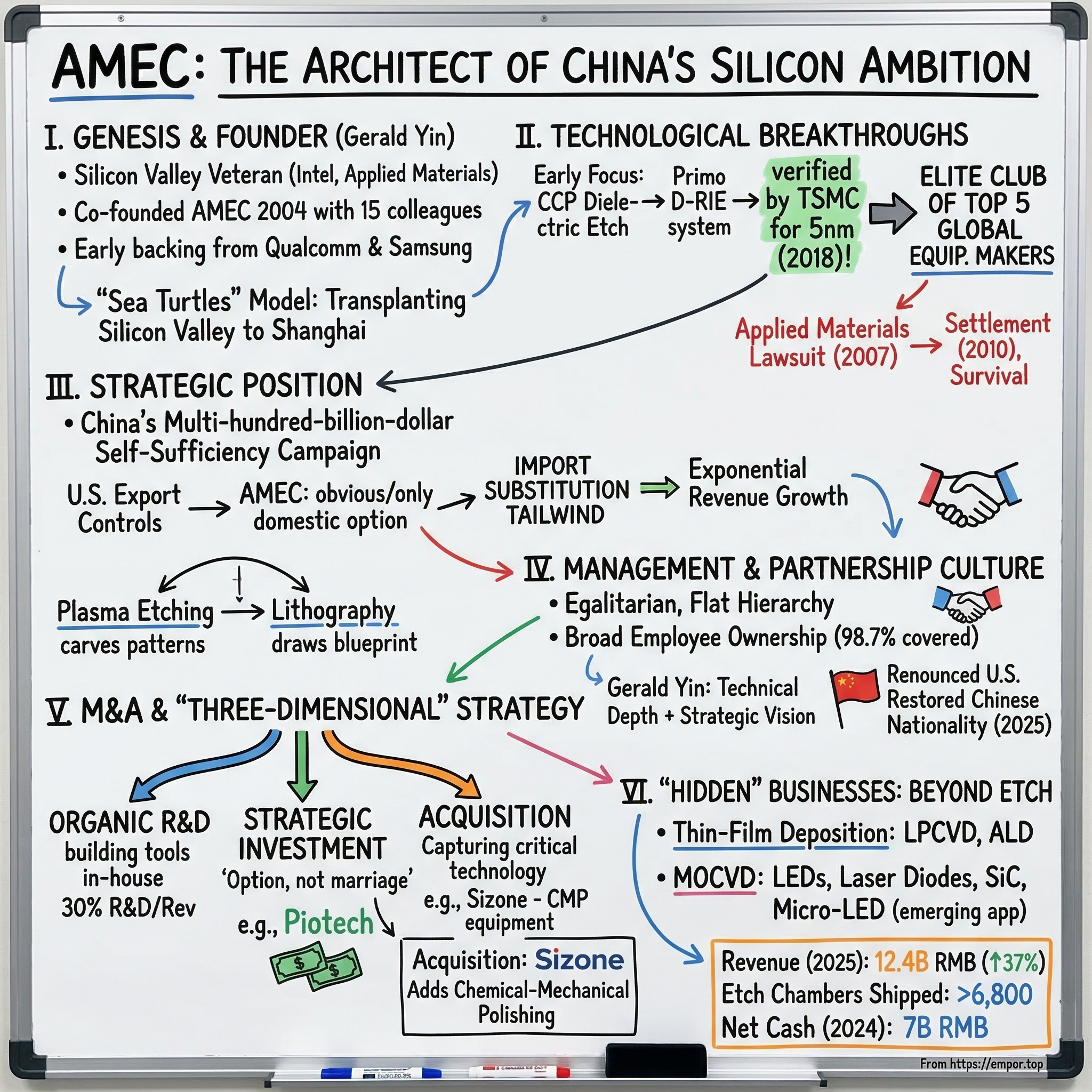
In April 2025, an 81-year-old man walked into a government office in Shanghai and did something that sent shockwaves through the global semiconductor industry. Dr. Gerald Zheyao Yin, the founder and chairman of Advanced Micro-Fabrication Equipment Inc. China—better known as AMEC—formally renounced his United States citizenship and restored his Chinese nationality. For a man who had spent over two decades building the etching tools that carved the digital age into silicon wafers at Intel and Applied Materials in Silicon Valley, this was not a bureaucratic formality. It was a declaration of allegiance in the most consequential technology war of the twenty-first century.
To understand why this moment mattered, you have to understand what AMEC actually does. Most people, even sophisticated investors, think of the semiconductor industry as a story about chip designers like Nvidia or foundries like TSMC. But there is a deeper layer—the companies that build the machines that make the chips. These are the true gatekeepers of the silicon economy, and there are shockingly few of them. Applied Materials, Lam Research, Tokyo Electron, ASML—these four firms collectively control the vast majority of the global semiconductor equipment market. For decades, no Chinese company came remotely close to challenging their dominance. Then AMEC arrived.
AMEC makes plasma etching equipment—the machines that use electrically charged gas to carve impossibly tiny patterns into silicon wafers. Think of it like this: if a chip is a miniature city, the lithography machine draws the blueprint, but the etching machine actually demolishes the buildings, digs the foundations, and carves the streets. Without the etcher, the blueprint is just a picture. At the scale AMEC operates, those "streets" are five nanometers wide—roughly one twenty-thousandth the width of a human hair, or about the length of twenty silicon atoms laid end to end. Getting that precision right, billions of times over, on a twelve-inch wafer, without a single defect ruining the chip, is one of the hardest engineering challenges humans have ever attempted.
The thesis on AMEC is deceptively simple but strategically profound: this is the company that broke the Western monopoly on advanced semiconductor etching equipment. In 2018, AMEC's tools were verified by TSMC—the world's most advanced chipmaker—for use in five-nanometer production. That single qualification placed AMEC into an elite club of perhaps five companies on earth capable of etching at the leading edge of physics. And it did so using what its founder calls a "Silicon Valley partnership model"—flat management, broad equity ownership, and a relentless focus on hiring the best engineers regardless of nationality—transplanted into the heart of Shanghai.
Today, AMEC trades on Shanghai's STAR Market under the ticker 688012.SS with a market capitalization of roughly 197 billion renminbi. In 2025, it generated 12.4 billion renminbi in revenue, a 37 percent increase over the prior year, and shipped more than 6,800 cumulative etching process chambers to fabs across the world. It is expanding aggressively into thin-film deposition, chemical-mechanical polishing, and power semiconductor equipment. And it sits at the epicenter of the most important industrial policy initiative in modern history: China's multi-hundred-billion-dollar campaign to achieve semiconductor self-sufficiency.
This is the story of how a sixty-year-old retiree from Applied Materials took fifteen colleagues back to Shanghai, survived a trade-secret lawsuit from his former employer, broke into the most exclusive supply chains on the planet, and built the company that may determine whether China can ever make advanced chips without Western permission.
II. The "Sea Turtle" Genesis and the 65nm Breakthrough
The story of AMEC begins not in a Shanghai laboratory, but in the sun-baked parking lots of Santa Clara, California, in the early 1980s. Gerald Yin arrived in Silicon Valley in 1984 with a Ph.D. in physical chemistry from UCLA and joined Intel's Central Technology Development group—the elite internal unit responsible for pushing Moore's Law forward. For a Chinese-born scientist in Reagan-era America, landing at Intel was the equivalent of a young physicist being invited to work at Los Alamos in 1943. This was where the future was being built.
Yin spent roughly two years at Intel before moving to Lam Research, where he co-invented the Lam 2300 series etch products—a platform that became an industry workhorse. But his most formative years came at Applied Materials, where he spent thirteen years rising to the rank of Corporate Vice President and General Manager of the Etch Product Business Group. At Applied, Yin didn't just manage engineers; he oversaw the development and commercialization of the etching tools that powered the transition from micron-scale to deep-submicron chip manufacturing. He later served as CTO of Applied Materials Asia, giving him a front-row seat to the explosive growth of chip fabrication in Taiwan, South Korea, and mainland China.
By the early 2000s, Yin was in his late fifties, wealthy, respected, and approaching the natural end of a distinguished American career. Then came the phone call that changed everything. A former middle school classmate—now a government official in China—invited Yin to consider returning home. The Chinese government, alarmed by its total dependence on foreign semiconductor equipment, was actively courting overseas Chinese scientists to come back and build a domestic industry. These returnees were called "hai gui"—"sea turtles"—a homophone for the Chinese word for "return from the sea." The metaphor was apt: like sea turtles that cross vast oceans to lay their eggs on the beach where they were born, these scientists were being called back to nurture something fragile and new.
In May 2004, at the age of sixty, Gerald Yin co-founded AMEC in Shanghai with fifteen former Silicon Valley colleagues. The venture attracted early backing from Qualcomm Ventures and Samsung—a signal that smart money in the global chip industry saw potential in a Chinese equipment startup, even at a time when the idea seemed quixotic. The founding team's pedigree was their calling card: collectively, they had hundreds of years of experience at the very companies whose monopoly they intended to break.
The early years were brutal. AMEC chose to start with CCP—Capacitively Coupled Plasma—etch technology, focusing specifically on dielectric etch. To understand why this mattered, consider that there are two main flavors of plasma etching. CCP etch uses an electric field between two parallel plates to generate plasma, and it excels at etching insulating materials like silicon oxide and silicon nitride—the "walls" and "insulation" of a chip's internal wiring. The other flavor, ICP—Inductively Coupled Plasma—uses a coil to generate a denser, more energetic plasma, and is better suited for etching the conductive materials like silicon and metal. AMEC's bet on CCP dielectric etch was strategic: it was a massive market, it was where the founders had deep expertise, and it allowed them to go head-to-head with Applied Materials and Lam Research on their home turf.
The gamble nearly ended in court. In 2007, Applied Materials filed a lawsuit alleging that AMEC—staffed by so many of its former employees—had used confidential information and trade secrets to develop its etching tools suspiciously quickly. The accusation was pointed: AMEC had built working etch and CVD systems within roughly a year of founding, a timeline that Applied argued was impossible without stolen intellectual property. The lawsuit hung over AMEC like a sword for three years, threatening to destroy the company before it ever reached commercial scale. In 2010, the two sides reached a settlement, agreeing to jointly own the disputed patent family. AMEC survived, but the experience left scars—and taught the company that in this industry, credibility was earned not just in the lab, but in the courtroom.
The breakthrough came when AMEC's Primo D-RIE system—its flagship dielectric etch platform—began winning acceptance at commercial fabs for 65-nanometer and 45-nanometer process nodes. These were not leading-edge nodes by the standards of the day, but they represented a psychological barrier. No Chinese equipment company had ever produced a tool that could meet the yield and reliability requirements of a production fab. The Primo D-RIE proved it could be done. Orders trickled in, then grew. AMEC won industry awards. More importantly, it won repeat orders—the ultimate validation that a tool works not just in a demo, but in the relentless grind of 24/7 high-volume manufacturing.
By the early 2010s, AMEC had shipped hundreds of CCP etch chambers and established itself as a credible, if still small, alternative to the Western incumbents. The company was generating meaningful revenue, attracting talent, and proving that the "sea turtle" model could produce real technology, not just PowerPoint presentations. But Gerald Yin knew that surviving at 65nm was not the same as winning. The real war would be fought at the leading edge, where the physics got harder, the tolerances got tighter, and the customers got infinitely more demanding. To reach that battlefield, AMEC would need a golden ticket—and that ticket would come from the most demanding customer in the history of semiconductor manufacturing.
III. The Inflection Point: The 5nm Golden Ticket
In the semiconductor equipment business, there is one validation that matters above all others: getting qualified by TSMC. Taiwan Semiconductor Manufacturing Company is not just the world's largest contract chipmaker; it is the world's most demanding customer. TSMC's engineers test equipment with a rigor that borders on the pathological—running thousands of wafers through qualification protocols, measuring yield down to individual defects per square centimeter, and demanding that tools perform identically across multiple chambers in multiple fabs. When TSMC qualifies a piece of equipment for a given process node, it is telling the world: "This tool works. We bet our most advanced production on it."
For AMEC, the TSMC qualification journey began at the 28-nanometer node, where the company's CCP etch tools were accepted into the supply chain. This was significant but not transformative—28nm was already a mature technology by the time AMEC gained entry. The real breakthrough came at 7nm, when AMEC became one of only five approved suppliers of etching equipment for TSMC's most advanced production line. Five companies on earth. AMEC was one of them.
Then came the moment that rewrote the narrative entirely. In late 2018, AMEC announced that its 5-nanometer plasma etching tools had been verified by TSMC. The implications were staggering. Five-nanometer represented the absolute frontier of semiconductor manufacturing—the node that would power the processors in Apple's iPhones, Qualcomm's flagship mobile chips, and the most advanced AI accelerators. For a Chinese company founded just fourteen years earlier to achieve parity with Applied Materials and Lam Research at this level was, in the words of one industry analyst, "like a minor-league baseball team winning the World Series."
The narrative around AMEC shifted overnight. Before the 5nm qualification, AMEC was discussed as a "cheap domestic alternative"—a company that might serve China's less demanding fabs but would never compete at the leading edge. After the qualification, AMEC became a "technological peer." The distinction matters enormously for long-term investors: a cheap alternative competes on price and eventually gets margin-squeezed; a technological peer competes on capability and earns the right to premium pricing.
It is important, however, to be precise about what AMEC's 5nm qualification means and what it does not. AMEC's tools were qualified for specific etch steps within the 5nm process flow—not for every etch step. A modern 5nm chip requires hundreds of individual etch steps, and different tools from different suppliers are used for different steps depending on the specific chemistry and geometry involved. AMEC's qualification meant it could handle certain dielectric etch steps at 5nm; it did not mean AMEC could single-handedly replace Lam Research or Applied Materials across the entire etch module. But even a partial qualification at 5nm was transformative, because it proved that AMEC's underlying technology platform—its plasma source design, its chamber engineering, its process control algorithms—could operate at the precision required by the most advanced nodes in existence.
The timing of this breakthrough was fortuitous in ways that Gerald Yin could not have predicted. In July 2019, AMEC listed on the newly created STAR Market—Shanghai's answer to Nasdaq—as part of the first batch of twenty-five companies to debut on the exchange. The IPO was priced at 29.03 renminbi per share, giving the company a price-to-earnings multiple of roughly 171 times. On its first day of trading, the stock surged 179 percent, closing near 81 renminbi and giving AMEC a market capitalization of approximately 43 billion renminbi. The STAR Market listing was not just a capital raise; it was a coronation. AMEC was dubbed the "top seed" of the STAR Market, and its IPO signaled to the world that China was serious about building a domestic semiconductor equipment industry.
The capital explosion could not have come at a better time, because the geopolitical landscape was about to transform AMEC from a niche equipment maker into a strategic national asset. The U.S.-China trade war, which escalated sharply in 2018 and 2019, created what might be the single most powerful tailwind in AMEC's history. As Washington imposed export controls on advanced semiconductor equipment, Chinese foundries like SMIC and Hua Hong faced an existential choice: find domestic alternatives or watch their technology roadmaps stall. Almost overnight, "import substitution" went from a nice-to-have to a survival imperative. AMEC, with its proven 5nm-capable etch tools, was the obvious—and in many cases the only—domestic option.
The paradox was exquisite. The same U.S. sanctions designed to hobble China's chip industry became AMEC's greatest growth accelerator. Every time Washington tightened restrictions on Lam Research or Applied Materials selling to Chinese fabs, AMEC's order book grew. The company went from competing for business to being pulled into fabs by desperate customers. Revenue, which had been roughly 2.2 billion renminbi in 2019, began its ascent toward the 12.4 billion it would reach in 2025—a nearly six-fold increase in just six years.
For investors, the STAR Market IPO and the trade war paradox together created a powerful flywheel: the IPO gave AMEC the capital to invest in R&D and manufacturing capacity; the trade war gave it the customers and order visibility to justify those investments; and each new tool qualification at an advanced node reinforced the narrative that AMEC was a technological peer, not a knockoff. The flywheel was spinning, and it was about to accelerate further.
IV. Management and the "Partnership" Culture
Walk into AMEC's headquarters on Taihua Road in the Pudong district of Shanghai, and the first thing you notice is what's missing: the rigid hierarchy that defines most Chinese state-adjacent enterprises. There are no executive dining rooms, no elaborate corner offices reserved for senior leaders, no visible caste system separating engineers from managers. Gerald Yin designed it this way deliberately, importing the egalitarian culture of a Silicon Valley startup into a country where corporate hierarchy often mirrors the bureaucratic layers of the state itself.
Yin's leadership style is an unusual hybrid. He has the technical depth of a lifelong process engineer—he still reviews experimental data from the lab and is known to challenge his R&D teams on the specifics of plasma chemistry. But he also has the strategic vision of a CEO who has spent two decades navigating the intersection of technology, geopolitics, and capital markets. At eighty-one years old, Yin remains AMEC's chairman and general manager, a level of longevity that is almost unheard of in the fast-moving semiconductor equipment industry. His continued presence signals both stability and a potential succession risk—a duality that investors must weigh carefully.
The most distinctive feature of AMEC's corporate culture is its approach to employee ownership. The company has implemented multiple equity incentive plans that, by the company's own disclosures, cover the vast majority of its workforce. The most recent restricted stock incentive plan, announced in 2025, targets executives, senior management, core technicians, board members, and—in a telling phrase—"other people who need to be motivated." In practice, this means that AMEC's approximately 2,480 employees are not just workers; they are co-owners. The company has described its employee stock ownership coverage as reaching 98.7 percent of eligible staff—a figure that, if accurate, would make AMEC one of the most broadly employee-owned technology companies in the world.
Why does this matter? Because in the semiconductor equipment industry, the scarcest resource is not capital, not patents, not even market access—it is people. Building a plasma etching tool that can operate at five nanometers requires a rare combination of expertise in plasma physics, materials science, vacuum engineering, process chemistry, and precision manufacturing. The engineers who possess this expertise are among the most sought-after professionals in the global technology industry, coveted by everyone from Huawei to well-funded startups backed by China's Big Fund. AMEC's broad-based equity ownership is its primary weapon in the talent war: it makes leaving financially painful and staying financially rewarding. When your stock has gone from 29 renminbi at IPO to over 300 renminbi in six years, the golden handcuffs are very real.
Gerald Yin's own financial alignment with shareholders is worth examining. His direct shareholding in AMEC is relatively modest—approximately 0.63 percent—but he also holds interests through management investment vehicles. More significantly, his 2025 decision to renounce U.S. citizenship was itself a form of alignment: by making himself a Chinese national, Yin eliminated any regulatory risk that he might be forced out of the company under U.S. "foreign person" restrictions on participation in Chinese semiconductor development. Two other AMEC executives with U.S. citizenship had already departed in response to the October 2022 Commerce Department rules that prohibited American citizens from working at certain Chinese chip facilities. Yin's response was not to leave, but to change his nationality—a move that was as much a strategic calculation as a personal one.
The executive team around Yin reflects AMEC's hybrid DNA. The senior leadership includes Haitao Gao as Group Vice President of Operations, Fang Liu as Deputy General Manager and Board Secretary, Weiwen Chen as Senior VP and CFO, and Matt Ruby as Group Vice President and Chief Legal Officer. The presence of Ruby—an American lawyer navigating Chinese corporate governance—underscores the bicultural nature of AMEC's management. This is a company that files its annual reports in Mandarin, hosts its shareholder meetings in Shanghai, but thinks in the language of Silicon Valley venture capital: equity incentives, flat org charts, R&D intensity, and customer-centric engineering.
The "Silicon Valley in Shanghai" ethos has a direct impact on how AMEC competes. In a traditional Chinese state-owned enterprise, decisions flow downward through layers of bureaucracy, and innovation is often driven by government directives rather than customer needs. At AMEC, engineers are empowered to make technical decisions at the bench level, product development is driven by customer roadmaps rather than Five-Year Plans, and failure in the lab is treated as data, not disgrace. This cultural difference is difficult to quantify in a financial model, but it shows up in outcomes: AMEC's pace of product development—from CCP to ICP to LPCVD to ALD—has consistently outpaced expectations, and its customer satisfaction scores, as reflected in repeat orders and expanding wallet share, suggest that fabs see AMEC as a genuine partner rather than a politically mandated supplier.
The risk, of course, is that this entire culture is built around one man. Gerald Yin is irreplaceable in the way that Steve Jobs was irreplaceable at Apple—not because no one else can do the job, but because the culture, the credibility, and the strategic vision all flow from a single source. AMEC has not publicly disclosed a succession plan, and investors should watch this issue closely. The company's ability to maintain its partnership culture and technical momentum beyond Yin's tenure will be one of the most important determinants of its long-term value.
V. M&A and the "Three-Dimensional" Strategy
Gerald Yin has a phrase he uses when describing AMEC's growth strategy: "three-dimensional expansion." The first dimension is organic R&D—building new tools in-house. The second is strategic investment—taking minority stakes in adjacent companies to access their technology and talent. The third is acquisition—buying companies outright when the technology is critical and the opportunity is ripe. Watching AMEC deploy capital across all three dimensions reveals a company that thinks more like a Silicon Valley venture fund than a traditional industrial conglomerate.
The most instructive case study is Piotech. In 2015, AMEC co-invested alongside China's National Integrated Circuit Industry Investment Fund—the legendary "Big Fund"—and a Suzhou-based venture fund, putting a collective 270 million renminbi into Piotech, a Shenyang-based maker of CVD and thin-film deposition equipment. The investment logic was straightforward: AMEC was an etch company, Piotech was a deposition company, and together they could offer Chinese fabs a broader domestic equipment solution. But AMEC treated the investment as an option, not a marriage.
In the summer of 2023, AMEC began selling its Piotech shares. Between May and August, the company offloaded approximately 1.256 million shares—about one percent of Piotech's outstanding stock—for total proceeds of roughly 520 million renminbi, booking an after-tax gain of approximately 406 million renminbi. That gain was a meaningful contributor to AMEC's 2023 net income, which reached 1.79 billion renminbi. Then, in January 2026, AMEC announced plans to reduce its Piotech holdings further, authorizing sales of up to 3.66 million additional shares with an estimated transaction value of around 1.4 billion renminbi.
Was Piotech a good investment? By any traditional venture capital metric, it was excellent—AMEC turned a minority stake acquired for a fraction of the eventual market value into hundreds of millions in realized gains while retaining strategic optionality. But the decision to sell is equally revealing. AMEC chose not to acquire Piotech outright, even though it could have provided a captive deposition equipment capability. Instead, AMEC decided to build its own thin-film deposition tools—LPCVD and ALD systems—internally, while monetizing the Piotech stake to fund that internal development. The message to investors: AMEC prefers to own its core technology rather than depend on affiliates, even profitable ones.
The pattern extends beyond Piotech. AMEC has made strategic investments across the "pan-semiconductor" ecosystem, including in companies focused on critical sub-components like vacuum pumps, radio-frequency generators, and specialty chemicals. The logic mirrors what Applied Materials did in the 1990s and 2000s: if you can't buy the best components from independent suppliers—because geopolitics might cut off your supply at any moment—you had better invest in building a domestic supply chain. For AMEC, this is not abstract strategy; it is existential risk management. Every critical component sourced from a Western supplier is a potential single point of failure in a world of export controls.
The most significant recent move in AMEC's capital deployment playbook came in December 2025, when the company announced plans to acquire Sizone Technology, a Chinese maker of chemical-mechanical polishing equipment. CMP is one of the essential process steps in semiconductor manufacturing—after each layer of material is deposited and etched, the wafer surface must be polished to atomic-level flatness before the next layer can be applied. By acquiring Sizone, AMEC would add a fourth major equipment category to its portfolio, joining etch, thin-film deposition, and MOCVD. The move follows the Applied Materials playbook almost exactly: own the customer relationship by offering a broader suite of tools, making it harder for competitors to displace you and easier to cross-sell new products into existing fab accounts.
AMEC is also investing heavily in physical infrastructure. The company established AMEC Semiconductor Equipment (Chengdu) Co., Ltd. as a new R&D and production base in southwestern China, with a facility expected to become operational by 2027. Combined with its existing Shanghai headquarters and its MOCVD facility in Nanchang, AMEC is building a geographically distributed manufacturing footprint that reduces concentration risk and positions it to serve the growing number of fabs being built across China's interior provinces.
The capital to fund all of this comes from an increasingly robust balance sheet. As of year-end 2024, AMEC held 7.8 billion renminbi in cash and cash equivalents, plus 834 million in short-term investments, against only 732 million in total debt. The company's net cash position of roughly 7 billion renminbi gives it enormous financial flexibility to pursue acquisitions, fund R&D, and build new facilities without diluting shareholders. For a company that was raising capital through an IPO just five years earlier, the speed of balance sheet transformation has been remarkable.
VI. The "Hidden" Businesses: Beyond the Etch
For most of its history, AMEC has been synonymous with one thing: plasma etching. Analysts covering the stock, investors evaluating the thesis, and competitors watching the market all defaulted to thinking of AMEC as "the Chinese etch company." That label is rapidly becoming obsolete, and the investors who understand why are the ones who will capture the next phase of value creation.
The first and most important shift is happening within the etch business itself. AMEC's original strength was CCP—Capacitively Coupled Plasma—etch, the technology used to carve insulating materials on a chip. But the semiconductor industry's relentless push toward more complex architectures has elevated the importance of ICP—Inductively Coupled Plasma—etch, which handles conductive materials and is critical for the high-aspect-ratio structures found in 3D NAND memory and advanced logic chips. To visualize the difference: if CCP etch carves wide, shallow trenches, ICP etch drills narrow, deep holes—like boring a tunnel through a mountain rather than digging a drainage ditch. As memory chips stack more layers vertically—current 3D NAND architectures exceed 200 layers—the "tunnels" get deeper and narrower, and the precision of ICP etch becomes the bottleneck for the entire manufacturing process.
AMEC launched its first ICP product, the Primo Nanova system, and the platform has since achieved a compound annual growth rate of over 100 percent in installed chambers. The Nanova series is now qualified for use in advanced memory and logic device designs, and by 2025, AMEC's ICP etch orders had grown to rival its legacy CCP business. Cumulative CCP etch shipments exceeded 4,500 reaction stations by mid-2025, but ICP was closing the gap fast. This transition matters for two reasons: first, ICP tools tend to carry higher average selling prices than CCP tools, which supports revenue growth even if unit volumes plateau; second, ICP qualification at advanced nodes deepens AMEC's competitive moat, because switching costs for ICP tools are extremely high—once a fab has qualified an ICP tool for a specific etch step in a 200-plus-layer NAND process, replacing it would require months of requalification and risk billions of dollars in yield loss.
The even more exciting growth story, however, is in thin-film deposition. In 2024, AMEC shipped its first commercial LPCVD—Low-Pressure Chemical Vapor Deposition—equipment, generating 156 million renminbi in revenue from what was essentially a standing start. The ramp was breathtaking: the company had shipped just one LPCVD unit in 2023; in 2024, it delivered 128 units. By 2025, cumulative LPCVD shipments surpassed 300 chambers, and the thin-film segment generated 506 million renminbi in annual revenue—a 224 percent increase over 2024. In the first three quarters of 2025 alone, thin-film revenue reached 403 million renminbi, up more than thirteen-fold year over year.
To put this in context: thin-film deposition is where layers of material are deposited onto the wafer before etching carves them into circuit patterns. If etching is the sculptor's chisel, deposition is the sculptor's clay. By offering both deposition and etch tools, AMEC can now sell a more complete solution to fab customers, increasing its revenue per fab and reducing the number of vendor relationships each customer must manage. This is the "platform" strategy that made Applied Materials the dominant force in semiconductor equipment: own more process steps, own more of the customer's spending.
AMEC is also expanding into ALD—Atomic Layer Deposition—a technology that deposits material one atomic layer at a time with extreme precision. ALD is essential for the thinnest films used in advanced transistor architectures, and AMEC's tungsten-series ALD products now cover all tungsten applications for memory devices. Customer verifications have been completed, positioning AMEC for volume shipments as memory makers continue to push the boundaries of 3D NAND stacking.
Then there is the MOCVD business—Metal-Organic Chemical Vapor Deposition—which represents AMEC's play in the "beyond-silicon" semiconductor world. MOCVD equipment is used to grow the epitaxial layers that form LEDs, laser diodes, and power semiconductor devices. AMEC's Prismo series—including the D-Blue for high-brightness LEDs, the HiT3 for deep ultraviolet LEDs, and the UniMax for mini-LEDs—has captured a leading share of the Chinese MOCVD market. The UniMax platform alone surpassed 100 chamber orders, a milestone that underscores AMEC's growing dominance in LED manufacturing equipment.
But the real option value in MOCVD lies in two emerging applications: silicon carbide power devices and micro-LEDs. Silicon carbide is the material of choice for the power inverters in electric vehicles—it handles higher voltages and temperatures than traditional silicon, enabling longer range and faster charging. As the EV industry scales globally, demand for SiC epitaxial equipment is growing rapidly, and AMEC's MOCVD expertise positions it to capture a meaningful share. Micro-LED, meanwhile, is widely viewed as the next-generation display technology—offering the brightness and efficiency of OLED with the longevity and scalability of traditional LEDs. AMEC signed an agreement with the Nanchang city government to establish an MOCVD R&D and production facility specifically focused on micro-LED technologies, betting that when the micro-LED market inflects, AMEC will be among the few companies with the equipment to serve it.
The MOCVD segment generated approximately 379 million renminbi in revenue in 2024, down roughly 18 percent year over year due to cyclical weakness in the LED market. This decline, however, masks the underlying strategic value: AMEC is building optionality in SiC and micro-LED that could become significant revenue drivers as those end markets mature. The current dip in MOCVD revenue is a function of the LED cycle, not a reflection of AMEC's competitive position.
Taken together, these "hidden" businesses are transforming AMEC from a one-product company into a multi-platform equipment supplier. In 2021, etch was essentially the entire revenue base. By 2025, thin-film and MOCVD combined contributed nearly a billion renminbi in revenue, and the growth trajectory suggests they could reach several billion within the next few years. For investors, the key insight is that the market still prices AMEC primarily as an etch company; the embedded optionality in thin-film, ALD, CMP, and MOCVD is largely unrecognized in the current valuation.
VII. Playbook: Business and Investing Lessons
There is a playbook that repeats throughout the history of semiconductor equipment, and AMEC is running it with remarkable discipline. The playbook has four chapters, and each one contains a lesson for investors thinking about the company's long-term trajectory.
The first chapter is the "platform" play. Applied Materials wrote this chapter in the 1990s when it expanded from etch and deposition into ion implantation, inspection, and eventually everything up to and including the tools that package finished chips. The logic is irresistible: every additional process step you offer increases your revenue per fab, deepens your customer relationships, and raises switching costs. AMEC is following this playbook with its expansion into LPCVD, ALD, CMP, and MOCVD. The Sizone acquisition for CMP equipment is the latest move, and it mirrors almost exactly the kinds of tuck-in acquisitions that Applied Materials used to build its empire. For investors, the question is not whether AMEC will become a multi-platform company—it already is—but whether it can maintain technical excellence across an increasingly broad portfolio without spreading itself too thin.
The second chapter is import substitution as a structural moat. In a world where the global semiconductor supply chain is bifurcating along geopolitical lines, being the "national champion" in a critical technology category provides a floor on revenue that global peers simply do not enjoy. When the U.S. government restricts Lam Research from selling advanced etch tools to Chinese fabs, those fabs do not stop manufacturing; they turn to AMEC. This creates a captive domestic market that functions as a guaranteed revenue base, insulating AMEC from the cyclical downturns that ravage Western equipment makers during industry slowdowns. The domestic replacement cycle in China—where local fabs systematically replace Western tools with Chinese alternatives—is a multi-decade tailwind that has no equivalent in the business models of Applied Materials or Tokyo Electron.
The third chapter is R&D as a competitive weapon. AMEC invested 3.7 billion renminbi in R&D in 2025—roughly 30 percent of revenue. That ratio is extraordinary by any standard. Applied Materials, by comparison, spends roughly 15 percent of revenue on R&D, and it is considered one of the most research-intensive companies in the semiconductor equipment industry. AMEC's R&D intensity reflects both necessity and ambition: necessity because it is still building out new product platforms that the Western incumbents developed decades ago; ambition because it is simultaneously pushing the frontier on advanced etch capabilities for nodes at 5nm and below. The company disclosed that it is developing more than twenty new equipment types across six equipment categories. For investors, the elevated R&D spend compresses near-term profitability—gross margins declined to roughly 39 percent in the first three quarters of 2025, down about three percentage points year over year—but it is building the product portfolio that will drive revenue growth for the next decade.
The fourth chapter is the partnership moat. Technology can be reverse-engineered. Patents can be worked around. Manufacturing processes can be copied. But a culture that makes 2,500 engineers feel like co-owners of a shared mission is extraordinarily difficult to replicate. AMEC's broad-based equity ownership, flat management structure, and Silicon Valley ethos represent a form of competitive advantage that does not show up on any balance sheet but is arguably more durable than any patent portfolio. In an industry where the cost of losing a single senior process engineer can set a product development program back by years, the ability to retain talent is not a "nice to have"—it is an existential capability.
The risk embedded in the playbook is execution. AMEC is attempting to do simultaneously what Applied Materials did sequentially over four decades: build multiple equipment platforms, achieve leading-edge technical capability in each one, and scale manufacturing to meet surging demand. The company is also navigating a geopolitical environment that adds layers of complexity—export controls, entity lists, nationality restrictions—that its predecessors never faced. History suggests that companies which try to do too much at once often stumble; the question for AMEC is whether the tailwinds of import substitution and government support are strong enough to overcome the headwinds of multi-front execution risk.
VIII. Analysis: 7 Powers and 5 Forces
To assess AMEC's competitive position rigorously, it is worth applying the analytical frameworks that separate superficial narratives from structural advantages.
Under Hamilton Helmer's 7 Powers framework, AMEC's most potent power is switching costs. Once an AMEC etch chamber is qualified in a fab's production line—particularly for an advanced node like 5nm or for a high-layer-count 3D NAND process—replacing it is not simply a matter of purchasing a competitor's tool and plugging it in. The replacement process requires months of requalification, during which the fab must run thousands of test wafers, validate yield at every step, and certify that the new tool produces identical results. For a fab running at full utilization, the opportunity cost of downtime during requalification can run into hundreds of millions of dollars. This creates an enormously sticky customer relationship: once AMEC is inside a production line, it tends to stay there, and each subsequent generation of the customer's technology is likely to use an upgraded version of the same AMEC tool rather than switch to a competitor.
AMEC's second power is what Helmer calls a cornered resource—in this case, the "sea turtle" management team. There is arguably no other group of people on earth who possess both the deep technical DNA of Silicon Valley semiconductor equipment development and the ability to navigate the Chinese regulatory, corporate, and political ecosystem. Gerald Yin's team combines Applied Materials-caliber process engineering with intimate knowledge of how to work with Chinese fabs, Chinese government agencies, and Chinese capital markets. This bicultural competence cannot be hired off a recruiting website or acquired through a merger; it was built over decades of lived experience on both sides of the Pacific.
The third relevant power is scale economies—though here AMEC's advantage is still emerging rather than fully established. AMEC's cumulative shipment base of over 6,800 etch chambers generates a growing pool of process data, customer feedback, and field reliability statistics that inform the design of next-generation tools. Each additional chamber installed in the field makes the entire platform marginally better, creating a learning curve that new entrants would struggle to replicate. However, AMEC's absolute scale remains far smaller than Applied Materials or Lam Research, which means the scale economy advantage is asymmetric: AMEC benefits from scale within China, but it does not yet enjoy the global scale advantages of the incumbents.
Turning to Porter's Five Forces, the picture is nuanced. The bargaining power of buyers is high—AMEC's customers include TSMC, SMIC, Hua Hong, and Samsung, all of which are massive enterprises with significant purchasing leverage. However, AMEC's position is strengthened by the fact that it is often the only domestic supplier capable of meeting advanced-node requirements, which limits buyers' ability to play suppliers against each other. In the Chinese market specifically, AMEC's bargaining position has been materially enhanced by U.S. export controls, which have reduced the number of available alternative suppliers.
The threat of new entrants is low. Building a semiconductor etch tool from scratch requires billions of dollars in R&D investment, years of development, and—most critically—access to fab partners willing to risk their production lines on an unproven tool. The qualification barrier alone is enough to deter most potential entrants. Within China, the only other meaningful domestic etch equipment maker is NAURA Technology, and the two companies compete in partially overlapping but distinct segments.
The threat of substitutes is essentially zero. There is no alternative to plasma etching in semiconductor manufacturing. Every advanced chip made anywhere in the world requires plasma etching at multiple steps in the fabrication process. Until some entirely new paradigm of chip manufacturing emerges—which no one in the industry expects within the foreseeable future—etching equipment will remain indispensable.
Supplier bargaining power is the most concerning force for AMEC. Many of the critical sub-components in an etch tool—radio-frequency generators, vacuum pumps, specialized ceramics, gas delivery systems—are sourced from Western or Japanese suppliers who may be subject to export controls. If Washington were to tighten restrictions on these sub-components, AMEC could face supply chain disruptions that would be difficult to mitigate in the short term. This is why AMEC has been investing aggressively in domestic component development and supply chain diversification—but the risk remains real and material.
Competitive rivalry within the global etch equipment market is intense but structured. Applied Materials, Lam Research, and Tokyo Electron compete fiercely for market share at global fabs, but the Chinese domestic market is increasingly walled off by export controls, creating a partially segmented competitive landscape in which AMEC and NAURA face less direct competition from Western incumbents than they would in an open market. This segmentation benefits AMEC but also limits its addressable market: if AMEC cannot sell tools to non-Chinese fabs at scale—whether due to customer reluctance, political risk, or technical gaps—its total addressable market is capped by the size of China's domestic semiconductor industry.
IX. The Bear vs. Bull Case
The Bear Case: The Geopolitical Glass Ceiling
The most compelling bear argument against AMEC is not about technology or execution—it is about geopolitics. AMEC's tools have been qualified at 5nm, but the path to 3nm and beyond requires not just better plasma sources and process control, but also access to sub-components and materials that may be restricted by Western export controls. If Washington decides to tighten the screws further—targeting, for example, the specialized ceramics, RF generators, or vacuum components that AMEC sources from Japanese and European suppliers—the company's technology roadmap could stall at a critical juncture.
There is also the question of subsidy dependency. AMEC has been a beneficiary of China's semiconductor investment ecosystem, including the Big Fund, which launched its third and largest phase in late 2024 with registered capital of 344 billion renminbi. Government support has provided AMEC with subsidized R&D funding, favorable tax treatment, and a policy environment that actively steers domestic fabs toward Chinese equipment suppliers. The bear case asks: what happens if the subsidies dry up? What if a future Chinese administration decides to reallocate semiconductor funding toward other priorities? AMEC's current revenue growth is partly organic and partly policy-driven; disentangling the two is difficult, and investors who assume the policy tailwind is permanent may be surprised.
The margin trajectory is another concern. AMEC's gross margin declined to roughly 39 percent in the first three quarters of 2025, down from about 42 percent the prior year, as the company ramped new product lines—LPCVD, ALD—that carry lower margins during their early scaling phase. R&D spending surged to 30 percent of revenue. The result is a company that is growing the top line at 37 percent but whose bottom-line growth of 31 percent lags revenue growth—a pattern that can only persist if the new products eventually achieve margin parity with the mature etch business. If they do not, AMEC risks becoming a company that grows revenue impressively but converts an ever-smaller share of that revenue into profit.
Finally, there is succession risk. Gerald Yin is eighty-one years old. He is the company's founder, chairman, chief strategist, and cultural touchstone. No succession plan has been publicly disclosed. The history of founder-led technology companies suggests that the transition to professional management is always difficult and sometimes catastrophic. Investors must price this risk, even if they cannot time it.
The Bull Case: The Dual Circulation Winner
The bull case for AMEC rests on a structural argument that transcends any single product cycle or quarterly result. China is the world's largest consumer of semiconductors, importing more than 300 billion dollars' worth of chips annually. The country's stated goal—reinforced by the "dual circulation" economic strategy and the ongoing U.S.-China technology competition—is to domestically produce a far greater share of the chips it consumes. Achieving this goal requires a massive expansion of domestic fab capacity, and every new fab needs etching equipment. Even if AMEC never sells another tool outside of China, the domestic replacement cycle alone represents a multi-decade growth opportunity that dwarfs anything available to its Western competitors.
The contract liability figure tells the story in financial terms. At the end of the third quarter of 2025, AMEC's contract liabilities—advance payments from customers for tools not yet delivered—stood at 4.39 billion renminbi, up 70 percent from the 2.59 billion at year-end 2024. This is the closest thing to a forward-looking order book that AMEC discloses, and it signals that demand continues to accelerate even as revenue grows at double-digit rates.
The bull case also points to AMEC's expanding product portfolio as a source of durable competitive advantage. By 2025, AMEC was no longer just an etch company; it was a multi-platform equipment supplier with products spanning CCP etch, ICP etch, LPCVD, ALD, MOCVD, and—pending the Sizone acquisition—CMP. Each new platform expands the total addressable market, deepens customer relationships, and increases switching costs. The analogy to Applied Materials' evolution from a single-product company to a diversified equipment conglomerate is apt, and Applied's trajectory provides a template for what AMEC's valuation could look like if the multi-platform strategy succeeds.
Perhaps most importantly, AMEC's 2024 legal victory against the U.S. Department of Defense demonstrated something that the market had been slow to recognize: AMEC is a commercial company, not a military entity. In January 2024, the Pentagon added AMEC to its Chinese Military Companies list—a designation that, if upheld, could have triggered investment restrictions and further export controls. AMEC responded by filing suit in U.S. District Court in August 2024, arguing that the Pentagon's designation was factually unfounded and violated due process. By December 2024, the Pentagon had rescinded the designation and removed AMEC from the blacklist. The lawsuit victory was more than a legal footnote; it established a precedent that AMEC is willing and able to defend its commercial reputation in Western courts, and that its business is driven by civilian technology demand, not military applications.
The bull case envisions AMEC as the "Tokyo Electron of China"—a national champion equipment maker that grows alongside its domestic semiconductor industry and eventually competes globally with the Western incumbents. Tokyo Electron, which today has a market capitalization exceeding 10 trillion yen, followed a similar trajectory in Japan during the 1980s and 1990s, growing from a domestic supplier into a global top-three equipment company. If AMEC can replicate even a fraction of that trajectory, the current valuation—roughly 197 billion renminbi, or about 27 billion U.S. dollars—could prove to be a compelling entry point.
The KPIs That Matter
For investors tracking AMEC's ongoing performance, three metrics deserve particular attention.
The first is contract liabilities growth, which serves as a proxy for forward order momentum. Because AMEC does not disclose a traditional order backlog in the way Western equipment companies do, the contract liabilities line—representing advance payments received from customers—is the best available indicator of future revenue visibility. The 70 percent year-over-year increase in Q3 2025 was a powerful signal; sustained growth in this metric would confirm that domestic demand continues to accelerate.
The second is R&D intensity as a percentage of revenue. At 30 percent in 2025, AMEC's R&D spend is nearly double the ratio of its Western peers. This is appropriate for a company building out new product platforms, but it cannot persist indefinitely without eroding returns. Investors should watch for this ratio to begin declining toward the 20 percent range as new products like LPCVD and ALD move from development to volume production, signaling that AMEC's investment phase is transitioning into a harvest phase.
The third is non-etch revenue as a percentage of total revenue. In 2025, thin-film and MOCVD combined represented roughly 7 to 8 percent of total revenue. If AMEC's platform strategy succeeds, this figure should rise steadily toward 20 percent or higher over the next several years, demonstrating that the company is successfully diversifying beyond its etch roots and building the multi-platform portfolio that will define its next growth chapter.
X. Epilogue and Final Reflections
In a fluorescent-lit courtroom in Washington, D.C., in the summer of 2024, the story of AMEC reached its most symbolically charged moment. A Chinese semiconductor equipment company—founded by a man who had spent his best professional years at the heart of America's technology establishment—stood before a U.S. federal judge and argued, successfully, that it was not a military threat. The Pentagon had placed AMEC on its Chinese Military Companies list based on what the company argued was a single, misinterpreted 2019 award, with no substantial evidence of any military affiliation. The court agreed. By December, AMEC was removed from the blacklist. The episode was a microcosm of the larger story: a company caught between two superpowers, fighting for the right to exist as a commercial enterprise in a world that increasingly sees technology through a military lens.
Gerald Yin's response to this pressure—renouncing his American citizenship, doubling down on R&D, expanding into new equipment categories, and suing the U.S. government—reveals a leader who understands that AMEC's survival depends on being indispensable to too many people on too many sides of the geopolitical divide to be easily eliminated. AMEC's tools etch chips that go into consumer electronics, automotive systems, industrial equipment, and telecommunications infrastructure across the world. Shutting AMEC down would not advance anyone's security interests; it would simply make chips more expensive and harder to get.
The financial record speaks clearly. Revenue grew from 3.1 billion renminbi in 2021 to 12.4 billion in 2025—a four-fold increase in four years. Net income rose from 1.0 billion to 2.1 billion over the same period. The cumulative etch chamber installed base surpassed 6,800 units. New product platforms in LPCVD, ALD, and CMP are scaling from zero to hundreds of millions in revenue. Contract liabilities are surging, indicating that the order pipeline continues to expand. And the balance sheet—with 7 billion renminbi in net cash—provides the financial flexibility to sustain investment through whatever geopolitical turbulence lies ahead.
AMEC is not without risk. Succession uncertainty, margin pressure from new product ramps, potential supply chain disruptions from tightened export controls, and dependence on government policy support are all real concerns that investors must weigh. But the structural position is formidable: AMEC is the domestic toll booth on China's semiconductor highway, and every chip fab built in China for the foreseeable future will need to pay the toll.
Gerald Yin once told an interviewer that when he left Silicon Valley in 2004, his former colleagues thought he was crazy. An established executive at the peak of his career, walking away from the most successful technology ecosystem in human history to start a semiconductor equipment company in a country that had never built one. Twenty-two years later, the tools that carry the AMEC logo etch patterns into silicon at five nanometers inside the cleanrooms of the world's most advanced chip fabs. The man who crossed the Pacific as a sea turtle has, against all odds, built something that the ocean cannot wash away.
 RSS Feed
 Spotify
 Apple Podcasts
 Amazon Music
 Audible
 YouTube