eMemory Technology: The Hidden Toll Road of the Semiconductor World
I. Introduction and Episode Roadmap
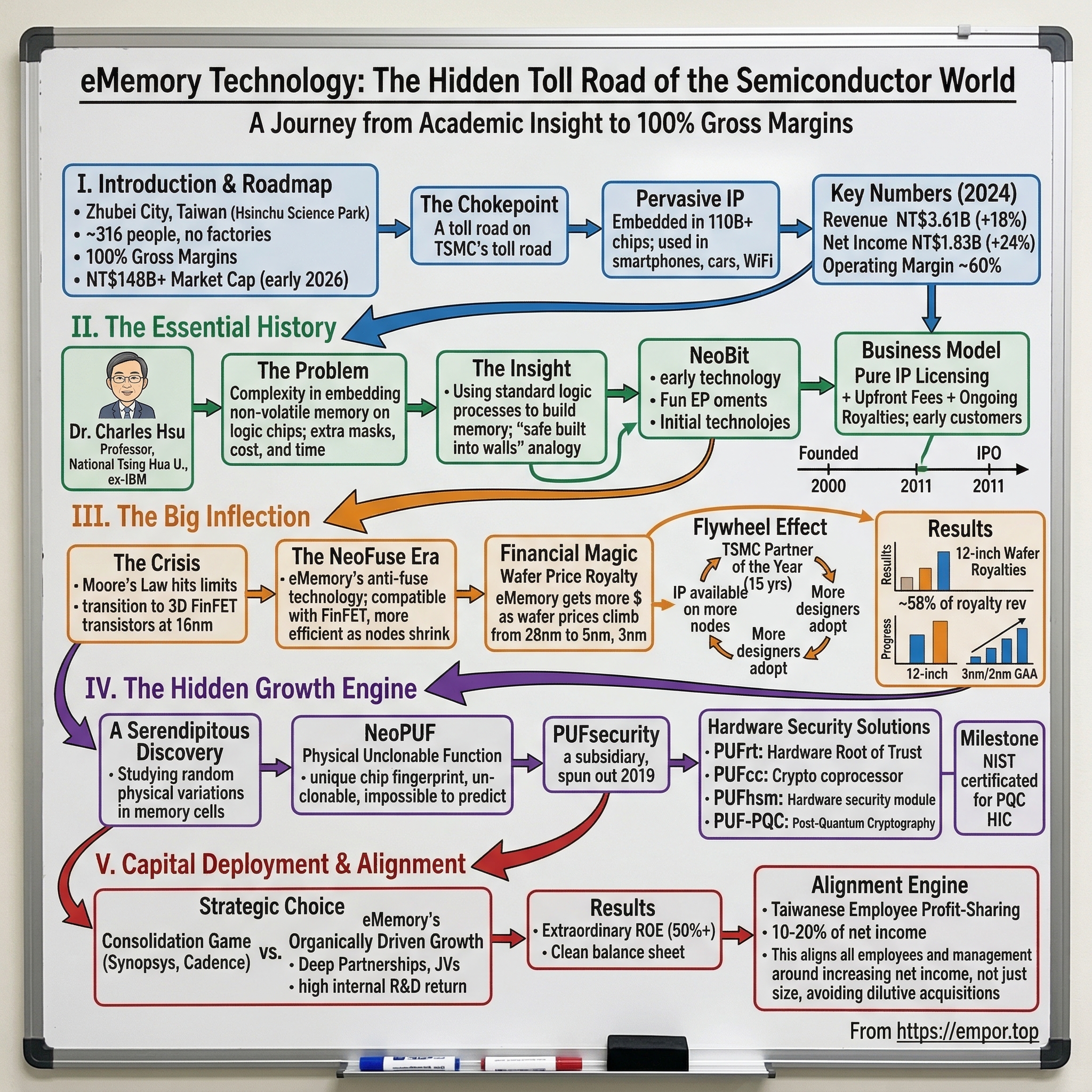
Somewhere in Zhubei City, Taiwan, nestled inside the Hsinchu Biomedical Science Park, sits a company that most investors have never heard of. It employs roughly 316 people. It has no factories, no assembly lines, no warehouses full of silicon wafers. And yet, as of early 2026, eMemory Technology commands a market capitalization north of NT$148 billion, roughly five to six billion US dollars. Its gross margins sit at a number that makes even the most seasoned software investors do a double take: one hundred percent.
That is not a typo. eMemory Technology reports gross margins of 100%.
To understand how that is possible, you need to understand what eMemory actually does, and why it sits at the most invisible, most irreplaceable chokepoint in the global semiconductor supply chain. If you have ever used a smartphone, driven a modern car, connected to a WiFi router, or interacted with any device powered by a chip manufactured at TSMC, there is a near-certain chance that eMemory's intellectual property was embedded inside it. The company's technology has been baked into more than 110 billion chips shipped worldwide, a number so large it becomes almost abstract.
The premise of this story is simple but powerful. TSMC is often described as the toll road of the semiconductor industry: every major chipmaker must pass through its foundries. But eMemory is the toll road on top of that toll road. It owns the patents and designs for the tiny, critical blocks of memory logic that must be embedded inside virtually every chip that rolls off TSMC's production lines. Every time a wafer is produced at an advanced manufacturing node, eMemory collects a royalty. The chip designer pays. The foundry facilitates. And eMemory's cash register rings, with zero marginal cost.
This is the story of how a professor and his graduate students in Taiwan turned an academic insight about embedding memory into logic circuits into one of the highest-quality business models in the global technology ecosystem. We will cover how they built the foundational relationship with TSMC that powers everything, how the physics of semiconductor miniaturization transformed them from a niche vendor into an indispensable ecosystem partner, how a serendipitous discovery in their labs spawned a cybersecurity subsidiary that could become their next massive growth vector, and why their disciplined refusal to play the acquisition game has created one of the most capital-efficient compounding machines in the industry.
The numbers tell a story of relentless improvement: revenue grew 18% in 2024 to NT$3.61 billion, net income surged 24% to NT$1.83 billion, and the company sports operating margins near 60% and net margins above 50%. But the real story is not in the financial statements. It is in the physics, the patents, and the ecosystem lock-in that make this business nearly impossible to replicate.
II. The Short, Essential History: Inventing Logic NVM
The year was 2000. Dr. Charles Hsu, a professor of electrical engineering at National Tsing Hua University in Hsinchu, had spent the previous eight years teaching and researching semiconductor memory devices. Before that, he had spent five years at IBM's legendary T.J. Watson Research Center in New York, where he had worked on the bleeding edge of semiconductor physics from 1987 to 1992. He held a PhD from the University of Illinois at Urbana-Champaign, one of the premier electrical engineering programs in the world, and had already accumulated an impressive body of research. By the late 1990s, he held dozens of patents and had published extensively on the behavior of memory cells at the transistor level.
But Hsu was not content to remain in academia. He saw a problem that the semiconductor industry was struggling with, and he believed his research team at Tsing Hua had cracked a solution.
The problem was this: as chips became more complex, designers increasingly needed small amounts of non-volatile memory, memory that retains its data even when power is turned off, to be embedded directly onto their logic chips. Think of it as a chip's personal notepad. It stores calibration data, security keys, chip identification codes, analog trim settings, and other critical parameters that the chip needs to function correctly from the moment it powers on. Without embedded non-volatile memory, every chip would need an external memory component, adding cost, board space, and design complexity.
The challenge was that traditional methods of embedding memory onto a logic chip were expensive and cumbersome. The standard approach required adding extra manufacturing steps, additional photolithographic masks, to the chip fabrication process. Each extra mask could add millions of dollars in development cost and weeks to the production timeline. For small and medium-sized chip designers, this was prohibitively expensive. For foundries like TSMC, which were building their business around offering standardized manufacturing processes to hundreds of different customers, the inefficiency was a major headache.
Hsu and his students developed a fundamentally different approach. Instead of requiring extra manufacturing masks, their technology, called NeoBit, used the standard logic manufacturing process itself to create memory cells. The key insight was elegant: by cleverly exploiting the physical properties of the transistors already being built on the chip, they could create memory storage without any additional process steps. No extra masks. No extra cost to the foundry. No extra complexity for the chip designer.
To use a simple analogy: imagine a construction crew building a house. The traditional approach to adding a safe would require bringing in a specialist team with special tools and materials. Hsu's approach was equivalent to showing the existing crew how to build a safe using only the bricks, mortar, and tools they were already using. Same construction process, same materials, but now you get a secure storage vault built right into the walls.
In 2000, Hsu gathered several of his graduate students and founded eMemory Technology. The company set up shop in Hsinchu, the epicenter of Taiwan's semiconductor industry, just down the road from TSMC's headquarters. By 2002, NeoBit had been qualified, licensed, and brought into production. The early customers were makers of LCD drivers, power management ICs, and other relatively simple chips manufactured on mature process nodes like 0.18-micron technology. These were not glamorous products, but they were high volume, and they proved the concept worked.
The business model that emerged was pure intellectual property licensing. eMemory did not manufacture anything. It designed the memory IP blocks, worked with foundries to qualify those blocks on their manufacturing processes, and then licensed the designs to chip companies. Revenue came from two streams: an upfront licensing fee when a customer adopted the IP into their chip design, and ongoing royalties paid for every wafer produced that contained eMemory's technology.
By 2011, the company had built enough traction to go public, listing on Taiwan's over-the-counter exchange under ticker 3529. But at this point, eMemory was still primarily a niche player focused on mature manufacturing nodes. The company was profitable and growing, but the explosive inflection point was still ahead. What changed everything was not a business decision. It was physics.
III. The Big Inflection: Advanced Nodes and The NeoFuse Era
In the early 2010s, the semiconductor industry was approaching a crisis point that most people outside the engineering world never heard about. Moore's Law, the observation that the number of transistors on a chip roughly doubles every two years, had been chugging along for decades. But as chipmakers pushed toward ever-smaller geometries, below 20 nanometers and then into the teens, the physics started to rebel.
The transistors themselves had to change shape. The flat, planar transistor design that had served the industry for decades could no longer contain the flow of electrons at these microscopic scales. Electrons were tunneling through barriers they were supposed to be blocked by. Current was leaking in places it was not supposed to leak. The industry's answer was a radical architectural shift: the FinFET transistor, a three-dimensional structure that wraps the gate around a thin fin of silicon, giving engineers much better control over the electrical current. TSMC introduced its first FinFET process at the 16-nanometer node in 2014, and the industry never looked back.
But here is what matters for our story: the traditional approaches to embedding memory on a chip, which already required extra manufacturing steps on planar processes, became even more problematic on FinFET. The physics of the new transistor architecture simply did not cooperate with legacy embedded memory techniques. Some approaches broke down entirely. Others became unreliable. The industry needed a new solution, and it needed one fast, because the most important customers in the world, Apple, Qualcomm, Nvidia, were all lining up to build their next-generation processors on these advanced nodes.
eMemory had been preparing for exactly this moment. Under the technical leadership of Dr. Rick Shen, who had been serving as president since 2009, the company had developed NeoFuse, a fundamentally new memory architecture based on anti-fuse technology. Where NeoBit had exploited the properties of standard transistors on mature nodes, NeoFuse used a different physical mechanism: it worked by selectively breaking down, or "blowing," a thin oxide layer to create a permanent electrical connection. This mechanism proved far more robust at the extreme miniaturization of FinFET processes.
The technical elegance of NeoFuse was that it was inherently compatible with the physics of shrinking transistors. As nodes got smaller, NeoFuse actually got more efficient, because the thinner oxide layers at advanced nodes required less energy to program. It was one of those rare situations in engineering where the trend that was breaking everyone else's technology was actively helping yours.
The timing aligned perfectly with a tectonic shift in the foundry business. TSMC was winning the Apple A-series processor business, one of the most coveted and highest-volume contracts in the semiconductor world. Apple demanded absolute reliability, and TSMC needed IP partners whose blocks would work flawlessly at high yield on its most advanced processes. eMemory, with NeoFuse qualified and proven on TSMC's cutting-edge nodes, became the de facto standard for one-time programmable memory on these processes.
This is where the financial magic happened. The economics of eMemory's royalty model undergo a phase change when you move from mature nodes to advanced nodes. Here is why: the cost of a single wafer at a mature node like 28-nanometer might be a few thousand dollars. But a wafer at TSMC's 5-nanometer node costs roughly $17,000, and at 3-nanometer, the price climbs even higher. eMemory's royalty is calculated as a function of wafer price. So as the industry migrated to more expensive advanced nodes, eMemory's royalty per wafer increased dramatically, without the company having to do anything differently. The IP block was already designed, qualified, and integrated. Every additional wafer was pure incremental revenue at essentially zero marginal cost.
The flywheel effect was powerful. As more chip designers adopted eMemory's IP on TSMC's advanced nodes, TSMC had even more incentive to prioritize qualifying eMemory on its newest processes, because doing so made TSMC's own platform more attractive to chip designers. And as eMemory's IP became available on more TSMC nodes, more designers adopted it, reinforcing the cycle. By the mid-2020s, over 770 of eMemory's silicon IP blocks had been deployed across TSMC's process technologies, and the company had won TSMC's Open Innovation Platform Partner of the Year award for an extraordinary fifteen consecutive years.
The migration to advanced nodes also shifted eMemory's revenue mix in a powerful way. Twelve-inch wafer royalties, which come predominantly from advanced nodes, grew to represent nearly 58% of total royalty revenue by mid-2024, up more than 37% year over year. Licensing revenue, which represents upfront design wins, grew over 22% in 2024, signaling a healthy pipeline of new designs that would generate royalties for years to come. The combination of growing wafer volumes at advanced nodes and rising wafer prices created a revenue engine that was scaling non-linearly, the kind of economics that makes compounders so powerful.
As of early 2026, NeoFuse has been qualified on TSMC's N3P process, the enhanced 3-nanometer node, and the company is actively working on qualification for 2-nanometer, which will mark TSMC's first adoption of the next-generation Gate-All-Around transistor architecture. Each new node represents another generation of lock-in, another layer of the toll road.
IV. The Hidden Growth Engine: PUFsecurity and The Cybersecurity Pivot
In the mid-2010s, something unexpected happened in eMemory's research labs. Engineers studying the behavior of their memory cells at the nanoscale level noticed something peculiar. Even when two memory cells were manufactured using the exact same process, on the exact same wafer, right next to each other, they exhibited tiny, random variations in their physical properties. These variations were not defects. They were the inevitable consequence of the quantum-level randomness inherent in the silicon manufacturing process: an atom here, an oxide thickness variation there. No two cells were ever exactly identical.
Most engineers would have dismissed these variations as noise, an annoyance to be compensated for in the design. But someone at eMemory had a different idea. What if those random variations were not a bug, but a feature? What if you could use the unique pattern of variations in a chip's memory cells as a kind of fingerprint, a physical identifier that was permanently embedded in the silicon itself, impossible to clone, impossible to predict, and impossible to fake?
This concept is known in the academic world as a Physical Unclonable Function, or PUF. The theory had been around since the early 2000s, but practical implementations had been elusive. The beauty of eMemory's discovery was that their existing memory cell technology, already embedded in billions of chips, naturally produced exactly the kind of random variations needed to create high-quality PUFs. They called their implementation NeoPUF, and it exploited quantum-tunneling mechanisms in the oxide layers of their memory cells to generate highly random, stable, and unclonable identifiers.
Think of it this way: when a snowflake forms, the underlying crystalline structure follows the same rules of physics, but every single snowflake is unique because of infinitesimal variations in temperature, humidity, and air currents during its formation. NeoPUF works on the same principle. Every chip's PUF pattern is unique because of the atomic-scale randomness in its manufacturing, and unlike a digital key stored in conventional memory, this fingerprint cannot be extracted, copied, or tampered with, because it is literally woven into the physical fabric of the silicon.
In 2019, eMemory made a strategic decision that signaled its ambitions extended well beyond memory IP. It spun out a subsidiary called PUFsecurity, dedicated to building complete hardware security solutions on top of the NeoPUF foundation. This was not just about selling a raw PUF IP block. PUFsecurity developed a full stack of security products: PUFrt, a Hardware Root of Trust that provides a secure foundation for chip identity and key management; PUFcc, a crypto coprocessor that handles encryption and authentication; PUFhsm, a hardware security module for managing cryptographic operations; and most recently, PUF-PQC, a post-quantum cryptography solution designed to protect against the future threat of quantum computers breaking today's encryption standards.
The timing of this pivot was prescient. The explosion of connected devices, from IoT sensors to autonomous vehicles to AI accelerators in data centers, has created an enormous and growing demand for hardware-level security. Software-based security can be patched and updated, but it can also be hacked and spoofed. Hardware-based security, rooted in the physical properties of the silicon itself, provides a fundamentally stronger foundation. Governments and industry standards bodies have been increasingly mandating hardware security features, and the automotive industry in particular has embraced hardware Root of Trust as a requirement for safety-critical systems.
PUFsecurity achieved a significant milestone when its PUF-PQC solution passed certification from the US National Institute of Standards and Technology for the latest post-quantum cryptography standards, including FIPS 205 and SP 800-208. This certification positions eMemory at the intersection of two massive secular trends: the proliferation of connected devices that need to be secured, and the looming arrival of quantum computing that threatens to break current cryptographic standards.
The strategic logic of the PUFsecurity subsidiary is elegant. It takes what was already an inherent byproduct of eMemory's core memory technology and transforms it into a new revenue stream in a much larger addressable market. The global hardware security market dwarfs the embedded memory IP market, and PUFsecurity gives eMemory a credible entry point. The subsidiary operates with the agility of a startup, pursuing design wins with automotive OEMs, IoT platform providers, and AI chip designers, while benefiting from eMemory's established relationships with every major foundry in the world.
Revenue from security-related IP has been growing at aggressive double-digit rates, though eMemory does not break out PUFsecurity's exact financials as a separate line item. What is clear from earnings call commentary and design win announcements is that this business is moving from early traction into a genuine growth vector. The partnership between PUFsecurity and Carota for secure over-the-air update solutions in automotive is one example of how the subsidiary is commercializing its technology in specific, high-value verticals.
For investors, PUFsecurity represents an embedded call option within the eMemory investment. If the cybersecurity business scales to even a fraction of its addressable market, it could meaningfully expand eMemory's total revenue base while maintaining the same asset-light, high-margin characteristics of the core memory IP business. The substrate is the same: designs licensed to foundries, royalties collected per wafer. Only now, the IP does double duty, providing both memory and security.
V. M&A, Capital Deployment, and The Anti-Acquisition Strategy
The semiconductor IP industry has been consolidating aggressively for over a decade. Synopsys, the $80-billion-plus behemoth, has grown into its current form through a relentless string of acquisitions, most notably its blockbuster deal for Ansys. Cadence Design Systems has followed a similar playbook, buying companies like OpenEye Scientific and Beta CAE Systems to broaden its offerings. ARM Holdings built its empire by acquiring smaller IP companies and folding their technology into its processor ecosystem. The prevailing wisdom in semiconductor IP is clear: buy, integrate, upsell, repeat.
eMemory has taken the opposite approach, and it has worked spectacularly.
The company has made virtually no significant acquisitions in its history. Its growth has been overwhelmingly organic, driven by internal R&D investment and the natural expansion of its technology into new process nodes and new use cases. This is not because eMemory lacks the financial resources to acquire. It generates substantial free cash flow and maintains a clean balance sheet with a debt-to-equity ratio of barely 1%. It is a deliberate strategic choice rooted in the economics of its business model.
The logic is straightforward. When your existing business generates operating margins near 60% and gross margins of 100%, the hurdle rate for any acquisition becomes almost impossibly high. Why buy a company at fifteen times revenue, take on integration risk, and potentially dilute your margin profile, when every dollar invested in internal R&D generates returns that are multiples higher? eMemory's R&D spending directly produces IP blocks that can be licensed across hundreds of foundry process nodes and thousands of customers, each generating royalties for years. The return on that internal investment is extraordinary.
Instead of acquisitions, eMemory has adopted a strategy of deep partnerships and strategic joint ventures. When the company needed to expand into RISC-V architecture support, it partnered with ecosystem players rather than acquiring a RISC-V company. When it needed to address the ARM ecosystem, it deepened its collaboration with ARM's design community. When it wanted to enter the hardware security market, it spun out PUFsecurity as a subsidiary rather than acquiring an external security company. Each of these moves preserved eMemory's margin profile while extending its reach.
The capital allocation implications are striking. Because eMemory does not spend its cash on acquisitions, and because its business requires minimal capital expenditure (no factories, no equipment, no inventory), the vast majority of its free cash flow is returned to shareholders. The company pays regular dividends and operates with the kind of capital efficiency that produces extraordinary returns on equity. ROE figures for eMemory have routinely exceeded 50%, and in strong years have pushed above 60%, putting it in the rarified company of the world's most capital-efficient businesses.
For context, a typical semiconductor company might generate ROE in the high teens or low twenties. A well-run software company might hit 30-40%. eMemory's sustained 50%+ ROE is a direct reflection of its asset-light model: high margins, low capital requirements, and disciplined avoidance of value-destroying acquisitions. It is the financial signature of a company that has resisted the empire-building temptation that derails so many successful technology firms.
The Taiwanese corporate governance framework reinforces this discipline in ways that are worth understanding. Under Taiwan's statutory employee profit-sharing system, a significant portion of net income, often 10-20%, is distributed directly to employees as profit-sharing bonuses. This creates a powerful alignment mechanism: employees and management benefit directly and immediately from profitability, not from the size of the corporate empire. There is no incentive to do a dilutive acquisition to "build scale," because building scale for its own sake does not increase the profit pool that gets shared. What increases the profit pool is higher margins, more design wins, and more royalty-generating wafers, exactly the metrics that align with eMemory's organic growth strategy.
VI. Current Management and The Alignment Engine
To understand how eMemory operates, you need to understand two very different people who complement each other almost perfectly.
Dr. Charles Hsu, the founder and chairman, is the visionary and the academic. He holds over 200 patents and has published more than 120 papers on semiconductor devices. He co-authored what is essentially the definitive textbook on logic non-volatile memory, a book published by World Scientific that distills two decades of research into the field he essentially created. Hsu thinks in terms of decades and fundamental physics. He is the person who identified the original opportunity in 2000, who saw that logic-process memory would become essential to the semiconductor industry, and who built the intellectual foundation that everything else rests on. He also sits on the board of Acer, reflecting his stature in Taiwan's broader technology ecosystem.
Dr. Rick Shen, the president, is the operator and the strategist. Where Hsu built the technology, Shen built the business. Shen joined eMemory after a stint as a principal engineer at TSMC, where he worked on manufacturing automation systems. This experience gave him something invaluable: a deep, first-hand understanding of how TSMC operates internally, what TSMC values in its partners, and how to navigate the complex qualification processes that determine whose IP gets embedded in TSMC's manufacturing flows.
After joining eMemory, Shen rose through a series of operational roles. He founded the customer service team, supervised technology and IP services, and oversaw the company's technology migration from 0.7-micron all the way down to 90-nanometer. He holds a PhD in electrical engineering from National Tsing Hua University, the same institution where Hsu had been a professor, and he personally holds over 80 patents and has co-authored 25 technical papers. When he became president in 2009, eMemory was still primarily a mature-node IP vendor. The transformation that followed, the aggressive push into FinFET and advanced nodes, the deep TSMC integration, the expansion into security, was executed under his operational leadership.
The Hsu-Shen partnership mirrors a pattern seen in many of the most successful technology companies: a visionary founder who understands the technology at its deepest level, paired with an operationally brilliant leader who can translate that vision into products, partnerships, and revenue. Hsu provides the long-term directional compass. Shen drives the day-to-day execution and the critical foundry relationships.
The broader management team operates within a Taiwanese technology compensation model that deserves attention because it explains a lot about eMemory's behavior. In Taiwan's statutory framework, companies are required to allocate a percentage of annual net income to employee profit-sharing. For technology companies like eMemory, this typically runs between 10% and 20% of net income, distributed as cash bonuses to employees. This is not a discretionary management decision or a board-approved bonus pool. It is baked into the corporate structure.
The effect on incentive alignment is profound. Every engineer, every manager, every executive at eMemory benefits directly when the company's net income grows. There are no golden parachutes for failed acquisitions because there are no acquisitions. There are no empire-building incentives because bigger is not necessarily more profitable. The system rewards exactly one thing: generating more net income from the existing business. And because eMemory's model is so leveraged to royalty growth on advanced nodes, the entire organization is aligned around the metrics that matter most: getting IP qualified on next-generation processes, winning design slots with high-volume customers, and ensuring that every qualified block translates into years of royalty streams.
Insider ownership at eMemory is robust. The executive team's personal wealth is meaningfully tied to long-term equity performance and dividend income, not to one-time transaction bonuses. This creates a management team that thinks like owners, because they functionally are owners. It is the kind of alignment structure that investor Warren Buffett has spent decades preaching about, and it occurs naturally within Taiwan's corporate framework rather than needing to be explicitly engineered through complex option packages.
The result is a management culture that is intensely focused, bordering on monastic. There are no press releases about entering new adjacent markets every quarter. There are no "strategic reviews" hinting at transformational M&A. There is simply a relentless focus on being the best in the world at logic non-volatile memory IP and building the security business on top of it. For a company with just 316 employees generating billions in revenue, this discipline is the invisible force multiplier.
VII. Frameworks: Hamilton's 7 Powers and Porter's 5 Forces
The best analytical frameworks are the ones that help explain why a business that looks too good to be true on paper can actually sustain those extraordinary economics for extended periods. eMemory is a case study in durable competitive advantage, and applying Hamilton Helmer's 7 Powers framework and Porter's 5 Forces reveals why.
Switching Costs: The Primary Power
This is the big one. Once eMemory's IP block is integrated into a chip designer's RTL (the hardware description code that defines a chip's logic), it becomes entangled with virtually every other element of the design. The memory block connects to calibration circuits, security modules, analog trim logic, and power management functions. Ripping it out and replacing it with an alternative is not like swapping one software library for another. It requires re-designing the affected circuits, re-running verification (which alone can take months), re-qualifying with the foundry, and re-taping out the chip, a process that for an advanced-node chip can cost $50 million or more just in mask costs.
No rational chip designer would take on that cost and risk to save a few cents per wafer on memory IP royalties. The switching cost is not just the financial expense; it is the schedule delay and the yield risk. In an industry where being six months late to market can mean losing an entire design cycle at Apple or Nvidia, the time cost alone makes switching unthinkable.
Network Economies and Ecosystem Effects
eMemory benefits from a powerful two-sided network effect. On one side, the more foundries that qualify eMemory's IP (TSMC, UMC, GlobalFoundries, Samsung, and others), the more attractive eMemory becomes to chip designers, because their designs become portable across manufacturing sources. On the other side, the more chip designers that standardize on eMemory's IP, the more foundries are motivated to qualify eMemory on their newest processes, because offering eMemory support makes the foundry's platform more attractive to designers.
This flywheel is self-reinforcing and extremely difficult for a competitor to replicate, because breaking in requires simultaneously convincing foundries to invest scarce engineering resources in qualifying unproven IP and convincing chip designers to take on the risk of adopting unqualified IP. Neither side wants to move first.
Cornered Resource
eMemory's patent portfolio around logic NVM and NeoPUF technology represents a genuine cornered resource. The company has accumulated hundreds of patents globally covering the fundamental mechanisms of logic-process non-volatile memory. These are not defensive patent thickets assembled through acquisition; they are original inventions that emerged from decades of focused research by Dr. Hsu, Dr. Shen, and their engineering teams. A competitor would need to invent around these patents, which constrains the available design space for alternative approaches.
Counter-Positioning
eMemory's pure-play, asset-light IP model creates a subtle but real counter-positioning advantage against larger competitors like Synopsys and Cadence. Those companies could theoretically develop competing embedded memory IP, but doing so would conflict with their strategic positioning as neutral EDA platform providers. If Synopsys aggressively pushed its own memory IP, it would risk alienating the IP vendors who are partners in its broader ecosystem. eMemory, as a pure-play specialist, has no such conflict.
Now applying Porter's framework:
Bargaining Power of Buyers: Low. eMemory's customers, the fabless chip designers, have limited leverage because eMemory's IP represents a tiny fraction of the total chip cost but serves a critical function. The royalty on a wafer might represent a fraction of a percent of the total wafer cost, making it economically irrational to push back aggressively on pricing. You do not negotiate hard on the cost of the screws when you are building a Ferrari.
Bargaining Power of Suppliers: Not Applicable. eMemory's primary inputs are the brains of its engineers. It does not depend on physical supply chains, raw materials, or manufacturing capacity. This is one of the fundamental advantages of a pure IP business model.
Threat of New Entrants: Extremely Low. To compete with eMemory, a new entrant would need to develop alternative logic NVM technology, convince a major foundry like TSMC to dedicate highly expensive and capacity-constrained R&D wafers to testing the unproven IP, survive the multi-year qualification process, and then persuade chip designers to adopt the new IP over the incumbent that has been proven in 110 billion chips. The barriers are not just high; they are practically insurmountable within any reasonable investment timeframe.
Threat of Substitutes: Low. The primary substitute for logic-process NVM is traditional embedded flash memory, which requires extra manufacturing masks and additional process steps. As chips move to more advanced nodes, embedded flash becomes increasingly difficult and expensive to implement, making eMemory's logic-process approach more advantageous with each new generation. The technology trend actively widens the moat.
Competitive Rivalry: Limited. The embedded NVM IP market has only a handful of meaningful players, primarily eMemory, Microchip (through its SST subsidiary), and to a lesser extent Synopsys. eMemory's dominant position on TSMC's advanced nodes, combined with its fifteen consecutive years as TSMC's IP Partner of the Year, gives it a competitive position that is more akin to a regulated monopoly than a contested market.
The combination of these forces explains why eMemory can sustain 100% gross margins and 50%+ net margins in an industry where most companies struggle to achieve half those numbers. The moat is not one single thing. It is the layered interaction of switching costs, network effects, patents, and the fundamental physics of semiconductor manufacturing, all reinforcing each other in a virtuous cycle.
VIII. The Bear vs. Bull Case and Future Outlook
The Bear Case
The most compelling bear argument against eMemory centers on concentration risk. The company's fortunes are deeply intertwined with TSMC. The vast majority of its advanced-node royalties flow through TSMC's foundries, and the TSMC relationship is the foundation upon which almost everything else is built. If TSMC were to lose significant market share, whether to Samsung's foundry division, to Intel's resurgent manufacturing ambitions, or to hypothetical future competitors, eMemory's royalty growth would decelerate.
This is not purely hypothetical. Intel has been investing tens of billions of dollars in its foundry services division, and Samsung continues to pour capital into advanced manufacturing. While TSMC's technological lead remains substantial as of 2026, the competitive landscape is not static, and a multi-year time horizon could see shifts that would impact eMemory's trajectory.
Geopolitical risk is the elephant in the room. eMemory is headquartered in Taiwan, its primary foundry partner is in Taiwan, and a significant share of its revenue originates from Taiwanese manufacturing activity. The geopolitical tensions surrounding Taiwan are well documented and need no elaboration here. What matters for investors is that eMemory has limited ability to diversify away from this geographic concentration because its competitive advantage is inextricably linked to its proximity to and integration with TSMC and the broader Taiwanese semiconductor ecosystem.
Then there is valuation. The market has long recognized the quality of eMemory's business model, and the stock consistently trades at premium multiples. The trailing P/E ratio routinely sits in the nosebleed range, pricing in years of continued growth. At these multiples, there is limited margin for error. If royalty growth disappoints for even a quarter or two, perhaps due to a cyclical downturn in semiconductor demand or a slower-than-expected ramp of a new process node, the stock could face meaningful compression. Investors are paying for perfection, and perfection is a high standard to maintain indefinitely.
A more subtle risk relates to PUFsecurity. While the security subsidiary represents an exciting growth opportunity, it is still in its relatively early stages, and the hardware security IP market is becoming increasingly competitive. Companies like Rambus, Intrinsic ID, and even the major EDA vendors are developing their own PUF and security solutions. PUFsecurity's success is not guaranteed, and if it fails to achieve commercial scale, the "embedded call option" argument weakens.
The Bull Case
The AI boom represents the most powerful near-term tailwind for eMemory, and the math is compelling. AI chips, whether Nvidia's GPUs, Google's TPUs, or the proliferating custom ASICs being designed by hyperscale cloud providers, are enormous, complex silicon devices manufactured on the most advanced (and most expensive) process nodes. They require extensive calibration memory, security features, and chip-ID functionality, all of which are eMemory's core competencies. As AI chip production scales, eMemory collects more royalties on more expensive wafers.
The advanced packaging trend amplifies this further. Modern AI chips increasingly use chiplet architectures, where multiple smaller dies are combined into a single package using advanced interconnect technologies like TSMC's CoWoS. Each individual chiplet within a package may require its own embedded NVM, creating multiple royalty events per package where previously there would have been one. More silicon surface area, more memory blocks, more royalties.
The secular migration from mature to advanced nodes provides a structural revenue tailwind that persists regardless of quarterly cyclicality. As 3-nanometer and eventually 2-nanometer processes ramp to high volume, they will constitute a growing share of eMemory's royalty base, and the per-wafer economics at these nodes are dramatically better than at older geometries. This creates a natural mix shift toward higher revenue per wafer, driving growth even if total wafer volumes are flat.
PUFsecurity's post-quantum cryptography certification positions eMemory at the forefront of a transition that every connected device on the planet will eventually need to make. As quantum computing advances from theoretical threat to practical concern, hardware security solutions that are quantum-resistant will shift from "nice to have" to "regulatory requirement." PUFsecurity's early positioning in this space could prove to be extraordinarily valuable.
Finally, the company's organic growth model means that every dollar of revenue growth falls through to the bottom line at exceptionally high incremental margins. There are no integration costs from acquisitions to absorb, no goodwill impairments to worry about, and no cultural friction from combining different engineering teams. Growth at eMemory is structurally more profitable than growth at almost any comparable technology company.
The KPIs That Matter
For investors tracking eMemory's ongoing performance, three metrics deserve focus above all others.
First, the royalty-to-licensing revenue mix. Royalties represent the recurring, high-margin annuity stream that drives the business. A steadily increasing royalty share of total revenue indicates that previous design wins are converting into production volumes, the ultimate validation of the business model. In recent quarters, royalties have represented roughly two-thirds of total revenue.
Second, advanced-node royalty penetration, specifically the percentage of royalties coming from 12-inch wafers on FinFET and GAA processes. This metric tracks the revenue mix shift toward higher-value wafers. As this percentage climbs, it signals that eMemory's revenue is becoming increasingly weighted toward the most expensive, fastest-growing segment of semiconductor manufacturing.
Third, PUFsecurity design wins. While the revenue contribution from security IP is still modest relative to the core memory business, tracking the number and quality of design wins at PUFsecurity provides an early signal of whether the security business is gaining the commercial traction needed to become a meaningful growth driver.
IX. Epilogue and Playbook Lessons
The semiconductor industry is one of the most capital-intensive on Earth. Building a leading-edge fabrication facility costs $20 billion or more. Designing a cutting-edge chip can run into the hundreds of millions. The physical infrastructure required to manufacture a single silicon wafer involves some of the most expensive and complex machinery ever created by human beings.
And yet, sitting quietly at the center of all this capital intensity is a company with 316 employees, no factories, no manufacturing equipment, and 100% gross margins, collecting a toll on virtually every advanced chip produced on the planet. eMemory Technology proves that in a world of massive physical infrastructure, the most valuable real estate can be intellectual.
The company's playbook offers several lessons that extend well beyond semiconductor investing. The first is the power of disciplined focus. eMemory has spent a quarter century doing essentially one thing: making logic-process non-volatile memory IP better, more reliable, and more compatible with the relentless march of semiconductor miniaturization. It has resisted the temptation to diversify into adjacent fields, to build its own chips, or to grow through acquisition. That discipline has allowed it to compound its advantage year after year, building switching costs and ecosystem integration that would take a competitor decades to replicate.
The second lesson is that the most valuable businesses are often the most invisible ones. eMemory's name appears on no consumer product. Its technology is never mentioned in the marketing materials for the chips it enables. Most of the engineers designing chips with eMemory's IP embedded in them probably do not think about it much, in the same way that you do not think about the foundation of a building while admiring its architecture. But remove that foundation, and the entire structure collapses.
The third lesson is about the economics of intellectual property in an era of escalating complexity. As semiconductor manufacturing becomes more expensive and more technically demanding with each generation, the IP that has been proven to work reliably at the most advanced nodes becomes exponentially more valuable. The cost of qualifying new IP on a 2-nanometer process is staggering, and the risk of failure is severe. This creates a powerful incumbency advantage for companies like eMemory that have already climbed the qualification mountain. Each new node is another layer of ice on the path behind them, making it harder for anyone else to follow.
A tiny company in Hsinchu achieved software-like economics in the middle of the world's most capital-intensive manufacturing industry. It did so not by building bigger, but by thinking smaller, all the way down to the quantum-level variations in individual silicon atoms that now serve as the foundation for its cybersecurity future. In the age of AI, where the conversation revolves around who builds the models, who designs the chips, and who manufactures the wafers, eMemory is a quiet reminder that sometimes the most powerful position in an industry is the one nobody can see.
X. Further Reading and Resources
- eMemory Technology Official Investor Relations page, including annual reports and earnings call transcripts, available at ememory.com.tw
- PUFsecurity product portfolio and NIST certification details at pufsecurity.com
- SemiWiki CEO Interview with Dr. Rick Shen, providing detailed insight into eMemory's advanced node strategy and TSMC partnership
- "Logic Non-Volatile Memory: The NVM Solutions from eMemory" by Dr. Charles Hsu, Yuan-Tai Lin, and Ching-Sung Yang, published by World Scientific, the foundational technical reference on the field
- TSMC Open Innovation Platform Partner Ecosystem documentation, detailing the qualification and integration process for IP partners
- Business Research Insights report on the Embedded NVM IP Market, covering market sizing, competitive landscape, and growth projections through 2035
- EE Times Asia feature: "eMemory Bets on Unique Encryption Tech," providing early coverage of the NeoPUF technology and its security applications
- National Institute of Standards and Technology FIPS 205 and SP 800-208 standards documentation, relevant to understanding PUFsecurity's post-quantum cryptography certification
- ChipEstimate technical article: "Optimal OTP for Advanced Node and Emerging Applications," a detailed technical overview of NeoFuse architecture and its behavior at advanced nodes
- Quartr investor relations platform coverage of eMemory Technology, including earnings call summaries and key financial metrics tracking
 RSS Feed
 Spotify
 Apple Podcasts
 Amazon Music
 Audible
 YouTube