Grand Process Technology (3131.TWO): The Wet Process Wizards of the AI Era
I. The Hook: The "Invisible" Bottleneck of the AI Revolution (0:00 - 0:10)
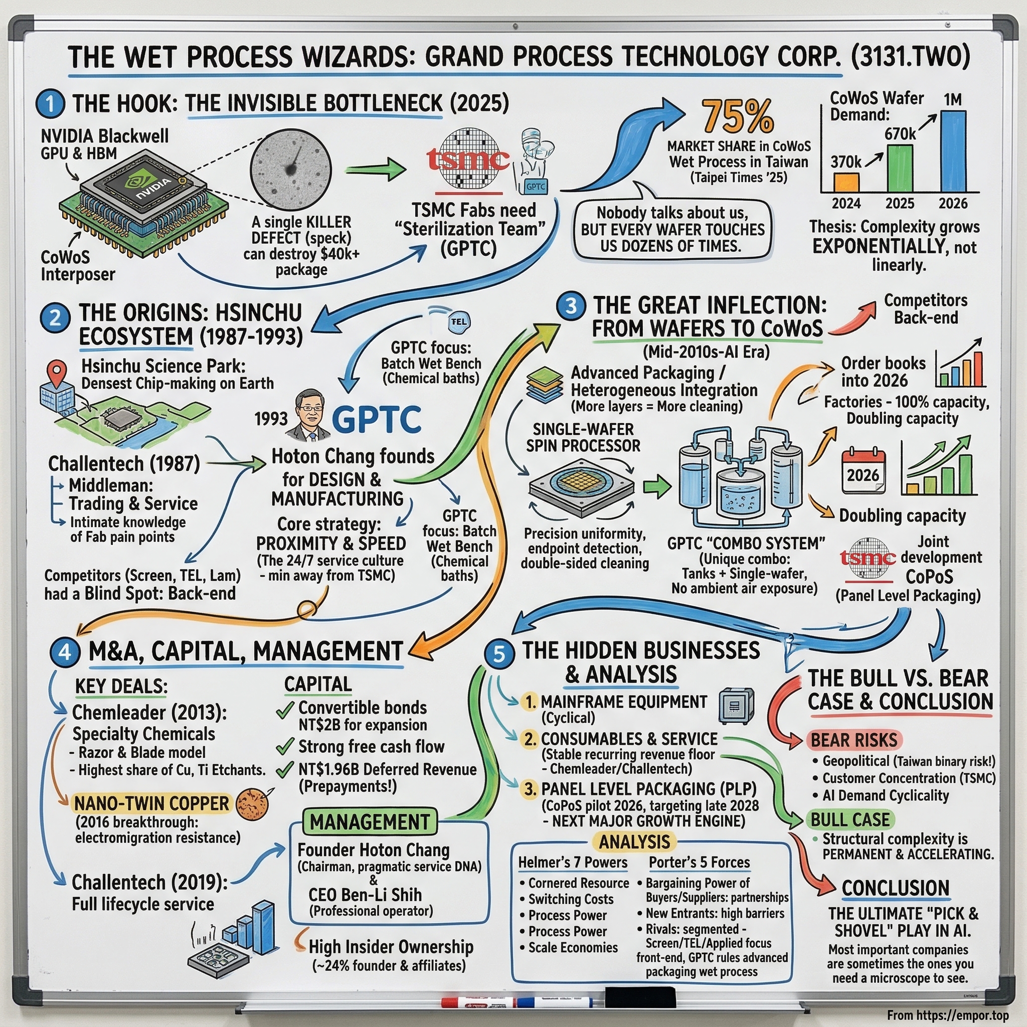
Picture this scene: it is late 2025, and inside a TSMC advanced packaging fab in southern Taiwan, a robotic arm lowers a 300-millimeter silicon wafer into a bath of precisely heated chemical solution. The wafer is worth tens of thousands of dollars at this point in the manufacturing process. Etched onto its surface are the redistribution layers that will eventually connect an Nvidia Blackwell GPU to its surrounding high-bandwidth memory stacks in an architecture known as CoWoS, or Chip on Wafer on Substrate.
If a single microscopic particle, invisible to the naked eye, survives this cleaning step, the entire multi-die package could fail. Billions of transistors, weeks of lithography, months of design work—all rendered scrap by a speck of contamination smaller than a virus.
That is not a hypothetical. In advanced semiconductor packaging, a single killer defect—one misplaced particle on a wafer surface—can destroy a chip package worth forty thousand dollars or more. The stakes at the nanoscale are brutal and unforgiving.
The world has spent the last three years obsessing over the right companies in the AI hardware stack. Nvidia designs the brains. TSMC prints the transistors. ASML builds the lithography machines that make the printing possible. SK Hynix stacks the memory.
But there is an invisible gatekeeper in this chain that almost nobody talks about—a company whose equipment touches every single one of those wafers dozens of times between process steps, ensuring that each surface is atomically clean before the next layer can be deposited, etched, or bonded.
That company is Grand Process Technology Corporation, ticker 3131 on the Taipei Exchange, and it operates under the group name HONSU.
Think of it this way: if TSMC is the surgeon performing the most delicate operation in industrial history, GPTC is the sterilization team. Nobody cheers for the sterilization team. Nobody writes breathless headlines about cleaning equipment. But if that team fails—if even one contaminant survives—the surgery fails. The patient is dead on the table.
What makes GPTC's story so compelling is not just that it makes cleaning equipment. It is that the company has quietly become the dominant supplier of wet process tools for the single hottest bottleneck in the entire AI hardware supply chain: TSMC's CoWoS advanced packaging lines.
According to a Taipei Times report from mid-2025, GPTC controls approximately seventy-five percent of the CoWoS wet process equipment market in Taiwan. That is a staggering concentration of market share in a process step that every major AI chip must pass through.
Here is a number that captures the magnitude of the opportunity: total global CoWoS wafer demand was estimated at 370,000 wafers in 2024, rose to approximately 670,000 in 2025, and is projected to reach one million wafers in 2026. Every single one of those wafers passes through ten to twenty or more wet process steps. Every one of those steps requires equipment that GPTC dominates. The math is almost embarrassingly straightforward.
The thesis is profound: as chips get more complex, as they move from single monolithic dies to multi-die packages stacked in three dimensions, the cleaning problem does not grow linearly. It grows exponentially.
More layers mean more process steps. More process steps mean more opportunities for contamination. More opportunities for contamination mean more cleaning equipment, more specialty chemicals, more precision.
And the company that understood this inflection point years before the market did—that pivoted from commodity batch cleaning tools to precision single-wafer systems for advanced packaging—is now sitting at the center of the most important supply chain on earth.
GPTC's revenue grew roughly sixty percent in 2025 to approximately NT$6.5 billion, around US$200 million. Earnings per share jumped from NT$28.89 in 2024 to NT$45.48, a fifty-seven percent increase. Its stock has roughly quadrupled since early 2024.
Its factories operated at one hundred percent capacity through the second half of 2025, and management disclosed that it could only fulfill half of customer demand. The company is now doubling its production capacity, has issued convertible bonds to fund expansion and M&A, and is jointly developing next-generation panel-level packaging equipment with TSMC itself.
This is the story of how a niche Taiwanese equipment maker, founded in 1993 in the shadow of the world's greatest foundries, became the indispensable janitor of the nanoscale. It is a story about the places where value hides in a technology supply chain, about the compounding power of deep customer relationships, and about why the most critical companies in the AI revolution are sometimes the ones you need a microscope to see.
II. The Origins: Finding a Lane in the Hsinchu Ecosystem (0:10 - 0:20)
To understand GPTC, you first have to understand Hsinchu. This modest city of about 450,000 people in northwestern Taiwan is, per square kilometer, arguably the most valuable patch of industrial real estate on the planet. The Hsinchu Science Park, established in 1980, is home to TSMC, UMC, MediaTek, and hundreds of smaller semiconductor companies that together form the densest and most sophisticated chip-making ecosystem ever assembled.
If Silicon Valley is where chips are designed, Hsinchu is where the world actually makes them.
By the late 1980s, the Hsinchu ecosystem was humming with an energy that had few parallels anywhere in the world. Taiwan's government had poured billions into the science park infrastructure, offering tax breaks, subsidized land, and research partnerships through ITRI, the Industrial Technology Research Institute, which had served as the original incubator for TSMC itself.
The result was an extraordinary clustering effect. Equipment vendors, chemical suppliers, wafer polishing companies, mask shops, and testing houses all crowded into the same few square kilometers, creating a web of just-in-time supply relationships that made the entire ecosystem operate like a single, highly optimized factory.
It was into this ecosystem that Hoton Chang, a Taiwanese entrepreneur with deep roots in the semiconductor equipment world, planted his first flag. In 1987, Chang founded Challentech International Corporation, a company focused on trading, representing, and servicing semiconductor equipment from foreign manufacturers.
This was not glamorous work. Challentech was essentially a middleman, importing tools from Japanese and American equipment makers and providing the installation, maintenance, and repair services that Taiwan's rapidly growing foundries needed.
But it gave Chang something invaluable: intimate knowledge of what the fabs actually required, where the pain points were, and which equipment categories were underserved by the foreign giants. He was not an outsider guessing at the market. He was the man whose technicians were inside the fabs every day, watching the production lines, listening to the process engineers complain about tool downtime, observing which cleaning steps caused the most yield losses.
This front-row seat to the inner workings of the semiconductor factory floor became the foundation for everything that followed.
By the early 1990s, Taiwan's semiconductor industry was entering its first major boom phase. TSMC, founded by Morris Chang in 1987, had proven the pure-play foundry model and was growing rapidly. UMC was expanding aggressively. And a constellation of packaging and testing houses, known as OSATs (outsourced semiconductor assembly and test), were springing up across Hsinchu and Kaohsiung. All of these fabs needed wet process equipment: the cleaning tanks, etching baths, and spin processors that chemically treat wafer surfaces between manufacturing steps.
The competitive dynamics of that era are worth understanding. The global semiconductor equipment market in the early 1990s was overwhelmingly dominated by Japanese and American companies. Tokyo Electron, Screen Holdings (then known as Dainippon Screen), and DNS had locked up the Japanese domestic market and were expanding aggressively into Taiwan. American giants like Applied Materials and Lam Research had established service offices in Hsinchu.
For a local Taiwanese company to compete against these entrenched players seemed almost presumptuous. The Japanese equipment makers, in particular, had decades of refinement behind their products, proprietary process know-how, and the credibility that came from serving the world's most demanding fabs.
But the foreign equipment makers had a blind spot. They were focused primarily on front-end wafer processing, where the margins were highest and the technology was most demanding. The back-end packaging and cleaning equipment market was smaller, less prestigious, and frankly beneath the strategic interest of companies chasing billion-dollar lithography and deposition tool orders.
The economics told the story: a front-end EUV lithography tool might sell for hundreds of millions of dollars, while a wet bench cleaning system sold for a few million. The multinational equipment makers naturally allocated their best engineering talent and their most aggressive sales efforts to the high-ticket items. Wet cleaning was a rounding error on their income statements.
This created a gap—and it was precisely the gap that Hoton Chang was positioned to exploit.
Here is a useful analogy for the non-technical reader. Imagine building a skyscraper. Between pouring each floor of concrete, you need to meticulously clean the surface, remove any debris, apply bonding agents, and verify that everything is perfectly level before the next pour. Now imagine doing this not with concrete but with materials only a few atoms thick, where a single grain of dust is a catastrophic defect.
Wet processing in semiconductors is that cleaning and surface preparation step—except the "skyscraper" is measured in nanometers and the "debris" is individual atoms.
The three main categories of wet processing are cleaning, etching, and stripping. Cleaning removes unwanted particles, organic residues, and metallic contamination from wafer surfaces using sequences of ultrapure chemical solutions. Etching uses carefully formulated acids to selectively dissolve specific material layers, carving circuit patterns with atomic precision. Stripping removes the photoresist polymer that served as a temporary mask during lithography, the step where patterns are transferred onto the wafer using light.
These sound simple in principle. In practice, they require extraordinary precision: the chemicals must be ultrapure, the temperatures controlled to fractions of a degree, and the process durations measured in seconds. Get any of those parameters wrong and the wafer is scrap.
In 1993, Chang made the leap from servicing other companies' equipment to designing and manufacturing his own. He founded Grand Process Technology Corporation, headquartered on Zhonghua Road in Hsinchu, literally minutes from TSMC's fabs.
The strategic logic was clear: Taiwan was becoming the center of global chip manufacturing, yet virtually all of the wet process equipment was being imported from Japan (Screen Holdings, Tokyo Electron) and the United States (Lam Research, Applied Materials). These foreign tools were expensive, their customization cycles were slow, and their service response times could not match the round-the-clock urgency of Taiwanese fab culture.
Chang bet on something that the larger competitors could not easily replicate: proximity and speed. When a TSMC process engineer identified a contamination issue at 2 AM, they did not want to file a service ticket with a company headquartered in Tokyo or Fremont and wait days for a field engineer to fly in. They wanted someone who could be at the fab in thirty minutes with a solution.
This culture of "24/7 service," of being physically embedded in the customer's backyard, became GPTC's founding competitive advantage.
This advantage deserves a deeper explanation because it is so often underestimated. In semiconductor manufacturing, tool downtime is measured not in inconvenience but in dollars per hour. A packaging line running high-value wafers might produce output worth millions of dollars per day. If a wet process tool goes down and the fab has to wait twelve hours for a Japanese service engineer to arrive, that is not just an annoyance; it is a direct hit to the bottom line.
GPTC's ability to have engineers on-site within hours, often minutes, was worth more than any technical specification advantage its foreign competitors might have claimed. "Speed of Hsinchu," as industry insiders call it, is not a marketing slogan. It is a measurable competitive advantage worth millions in avoided downtime.
The early years were defined by batch wet bench systems—the workhorses of wet processing. These are essentially sophisticated chemical baths: a series of tanks filled with precisely controlled solutions into which cassettes of twenty-five wafers are dipped, soaked, rinsed, and dried. Batch systems are high-throughput and cost-effective, ideal for standardized cleaning steps where dozens of wafers can be processed simultaneously.
GPTC built these systems for touch panel manufacturers, LED producers, and the less demanding back-end packaging lines of the era. It was bread-and-butter work, profitable but unremarkable. Nobody was writing analyst reports about it.
But Chang was quietly building something more valuable than any single product line. Through Challentech's service operations, his team was accumulating deep process knowledge: the specific chemical recipes, temperature profiles, agitation patterns, and rinse sequences that each customer used to achieve the yields they needed.
In semiconductors, these recipes are closely guarded intellectual property, and the equipment maker who understands them occupies a privileged position. You cannot replicate decades of accumulated process intelligence by hiring a few engineers or reading a manual. It lives in the institutional memory of the organization.
The company listed on Taiwan's Emerging Stock Market around 2008, then graduated to the Taipei Exchange (TPEX) on January 17, 2011. At the time, GPTC was a solid but unspectacular local equipment maker with annual revenue around NT$2 billion, profitable but not growing explosively.
Nobody confused it with Screen Holdings or Tokyo Electron. The stock was thinly traded, covered by virtually no sell-side analysts, and held almost entirely by domestic Taiwanese investors. It was the kind of company that institutional investors might glance at during a screening exercise and immediately move past—too small, too niche, too illiquid, no English-language coverage.
But the foundation had been laid: a vertically integrated group with equipment manufacturing capability, deep customer relationships, and a founder who had been studying the industry's trajectory for a quarter century. The question was whether the industry would ever create a moment where those advantages could be leveraged into something transformational.
For fifteen years, the answer had been no. The wet process equipment market was mature, the growth was incremental, and the returns, while steady, were unremarkable. Then the AI revolution arrived, and everything changed.
III. The Great Inflection: From Wafers to CoWoS (0:20 - 0:40)
For most of the semiconductor industry's history, the action, the prestige, and the investment dollars were concentrated at the "front end" of the manufacturing process. This is where transistors are actually formed on bare silicon wafers using lithography, deposition, etching, and ion implantation.
Front-end processing is where ASML's extreme ultraviolet lithography machines operate, where Applied Materials and Lam Research earn the bulk of their revenue, and where TSMC achieves its famous process node leadership—from 7 nanometers to 5 to 3 and now approaching 2 nanometers.
The "back end," by contrast, was historically the less glamorous cousin. This is the stage where finished die are cut from the wafer, packaged into protective housings, connected to substrates, and tested. For decades, back-end packaging was a relatively commoditized process: take a single die, attach it to a lead frame or substrate with wire bonds, seal it in epoxy, and ship it. The equipment was cheaper, the margins were thinner, and the innovation pace was slower.
Then, in the mid-2010s, something fundamental began to change. Moore's Law, the long-standing observation that transistor density doubles roughly every two years, started running into physical limits. Making transistors smaller was becoming exponentially more expensive with each new process node.
The industry's response was a paradigm shift that is still unfolding: instead of making one bigger, more complex chip, start connecting multiple smaller chips together in a single package. This approach, broadly known as "advanced packaging" or "heterogeneous integration," allowed chipmakers to combine compute dies, memory, input/output interfaces, and other functional blocks from different process nodes into a single high-performance unit.
The breakthrough technology that made this practical at scale was TSMC's CoWoS, which stands for Chip on Wafer on Substrate. Understanding CoWoS is essential to understanding GPTC's transformation, so it is worth explaining carefully.
Imagine you have several small puzzle pieces, each manufactured separately, that you want to connect together on a shared platform so they can communicate at extremely high speeds. These puzzle pieces are individual silicon chips, or "chiplets": a GPU die here, a stack of high-bandwidth memory there, perhaps an input/output controller on the other side.
In the CoWoS process, these chiplets are placed side by side on a large silicon interposer—essentially a thin wafer with an incredibly dense network of tiny wires embedded in it, like a miniature freeway system for electrical signals. The interposer connects the chiplets to each other with thousands of parallel data lanes running at speeds impossible with conventional packaging. The whole assembly then sits on a substrate that connects it to the circuit board.
To appreciate why wet processing becomes exponentially more critical at advanced packaging nodes, consider what contamination actually looks like under a scanning electron microscope.
At the scale of CoWoS redistribution layers, where copper traces are only a few micrometers wide and the gaps between them are even narrower, a contamination particle of just one hundred nanometers—roughly one-thousandth the width of a human hair—can bridge two adjacent copper lines and create a short circuit.
Under an electron microscope, these "killer defects" appear as irregular blobs sitting across meticulously patterned parallel lines, like a boulder dropped across a set of railroad tracks.
The physics compounds at every level. As feature sizes shrink, the ratio of surface area to volume increases dramatically, meaning surface contamination has proportionally more impact. A particle that would be harmless on a 28-nanometer chip becomes lethal when it lands on a CoWoS interposer where the pitch between copper lines has been reduced by an order of magnitude.
There is also the material complexity problem. CoWoS interposers combine copper, silicon dioxide, silicon nitride, tantalum, titanium, organic dielectric polymers, and solder alloys, all layered within micrometers of each other. Each material has different surface chemistry, different adhesion properties, and different sensitivity to chemical residues. A cleaning recipe that works perfectly for copper surfaces can corrode titanium barriers if the chemistry is not precisely controlled.
This is why the accumulated recipe knowledge matters so much: the cleaning must be chemically selective, removing contaminants while leaving the underlying materials untouched.
Why does this matter so much for wet process equipment? Because of the sheer number of chemical processing steps involved.
The silicon interposer alone requires multiple metal layers, each built through a repeating cycle: deposit a thin seed layer of metal, coat it with photoresist, pattern the photoresist with light, electroplate copper into the pattern, strip away the resist, and etch off the excess metal. At each transition between these steps, the wafer must be chemically cleaned.
The redistribution layers that connect the chiplets to the interposer require their own set of metal deposition, patterning, plating, stripping, and etching cycles. The under-bump metallization that creates the tiny solder connections requires yet more chemical processing. And after the chiplets are bonded, the carrier wafer used during processing must be cleaned and recycled.
Add it all up, and a single CoWoS wafer passes through ten to twenty or more discrete wet process steps. Compare that to traditional single-die packaging, which might involve only two or three cleaning steps. If the number of wet process steps per package triples and the total number of packages produced quadruples, the demand for wet process equipment grows by roughly twelve times.
That is the magnitude of the opportunity GPTC was positioned to capture.
CoWoS was first introduced by TSMC around 2012, but it remained a niche technology for years, used primarily in high-end FPGAs from Xilinx. The volumes were small, the economics marginal, and the packaging engineers were still refining the process.
Then came the AI revolution. When Nvidia designed its A100 and subsequently its H100 GPU for training large language models, it became clear that the only way to achieve the necessary memory bandwidth was to place the GPU die directly adjacent to stacks of high-bandwidth memory on a CoWoS interposer. Suddenly, CoWoS went from a curiosity to the critical bottleneck of the entire AI hardware supply chain.
The demand explosion was staggering. TSMC's CoWoS capacity stood at roughly 35,000 wafer equivalents per month in late 2024. By the end of 2025, it had more than doubled to approximately 75,000 wafers per month. The target for the end of 2026 is 130,000 to 150,000 wafers per month—a nearly fourfold increase in just two years.
Nvidia alone secured an estimated sixty percent of TSMC's total 2026-2027 CoWoS capacity to support its transition from the Blackwell architecture to the next-generation Rubin platform. The Rubin R100 GPU will use an even more advanced variant called CoWoS-L, which employs small silicon "bridge" chiplets instead of unified interposers, enabling package sizes approaching six times the standard reticle limit.
TSMC has been building massive new packaging facilities to meet this demand, and the scale of construction is worth enumerating because each new building represents a discrete wave of equipment orders for GPTC.
The AP7 complex in Chiayi is set to become the world's largest advanced packaging hub, with up to eight production buildings spanning a campus that dwarfs many of TSMC's existing wafer fabs. Phase 2 began equipment installation with production expected in 2026; Phase 1 is scheduled for mass production in 2027. The sequencing may seem counterintuitive—Phase 2 before Phase 1—but it reflects TSMC's urgency to bring any available capacity online as quickly as possible.
The AP8 facility in Tainan, repurposed from a former display plant, began mass production in the second half of 2025. An Arizona-based packaging hub is also under development, tied to TSMC's broader US manufacturing strategy and the CHIPS Act subsidies. This facility represents GPTC's potential entry into serving TSMC outside of Taiwan, though the logistics and service model would need to be adapted.
The Arizona facility is particularly interesting from a strategic perspective because it could force GPTC to establish its first significant overseas service presence—a step that would test whether the "Speed of Hsinchu" advantage can be replicated eight thousand miles from home.
ASE Technology, the world's largest OSAT, is tripling its monthly CoWoS output to 20,000-25,000 wafers by late 2026. Every one of these facilities needs wet process equipment.
This is where GPTC's technical evolution becomes the crucial plot point of the story. In the earlier era of simple packaging, batch wet benches were sufficient. You could dip twenty-five wafers at once into a chemical bath, and as long as the chemistry was roughly right, yields were acceptable.
But CoWoS interposers have feature sizes measured in single-digit micrometers, with copper wiring only a few micrometers wide and metal layers stacked with tolerances of less than a micrometer. At these dimensions, batch processing—where all wafers share the same chemical bath and contamination can migrate from one wafer to another—becomes an unacceptable yield risk.
GPTC's critical technical pivot was the development and commercialization of single-wafer spin processors for advanced packaging applications. In a single-wafer system, chemicals are dispensed directly onto each wafer individually while it spins at precisely controlled speeds.
This provides dramatically better uniformity, allows precise endpoint detection (the system can detect exactly when the etch reaches the target depth and stop automatically, avoiding over-etching), enables double-sided cleaning, and eliminates cross-contamination between wafers.
GPTC also developed its signature "combo system," which integrates soaking tanks and single-wafer spin chambers in a unified platform. This hybrid approach was specifically designed for the workflow of advanced packaging, where a wafer might need to soak in one chemical bath for a timed immersion and then immediately receive a precision spin etch in the same system, without being exposed to ambient air between steps.
The combo system is a uniquely GPTC innovation that has no direct equivalent from the major global competitors, who tend to sell batch tools and single-wafer tools as separate product lines.
This was the moment GPTC moved from "commodity" to "critical." The company was no longer selling generic cleaning tanks. It was selling precision tools whose recipes—the exact combination of chemical concentrations, spin speeds, dispense patterns, and endpoint detection parameters—were deeply integrated into the production process flows of the world's most advanced packaging lines.
And because GPTC had spent decades building relationships with TSMC, because its engineers understood the specific requirements from years of collaborative on-site work, it held a position that foreign competitors could not easily replicate from Tokyo or Fremont.
By mid-2025, the result was unmistakable. Order books stretched into the second half of 2026, with lead times extending well beyond the typical six-to-nine month delivery period. Vice President Travis Liang stated publicly that the company "sees no clear signs of an AI bubble" and expected operations to "continue to thrive over the next three to five years."
Equipment shipments reached 170-200 units in 2025, roughly double the prior year. The company that had spent two quiet decades building cleaning equipment for touch panels and LED factories had become a linchpin of the AI hardware stack—and the opportunity was still accelerating.
IV. M&A and Capital Deployment: The "Smart Money" Analysis (0:40 - 0:55)
One of the more revealing ways to evaluate a company's strategic intelligence is to examine not just what it builds organically, but what it chooses to acquire and when. In GPTC's case, the acquisition record is sparse by global standards—just two major deals over three decades—but both were surgically precise and both strengthened the company's competitive position in ways that continue to compound.
The first and arguably most important acquisition was Chemleader Corporation, which became a wholly owned subsidiary in 2013. Chemleader had been established in 2002 as part of the broader HONSU ecosystem, a specialty chemical company focused on developing and manufacturing the etchants, strippers, and electroplating chemicals used in wet processing.
At first glance, an equipment maker buying a chemical company might seem like a lateral move rather than a transformative one. But the strategic logic was brilliant and can be understood through a simple analogy: imagine an inkjet printer manufacturer acquiring its own ink company. The equipment creates the installed base; the chemicals create the recurring revenue stream.
Every GPTC wet bench and spin processor in the field consumes chemicals on an ongoing basis, and by owning the chemical supplier, GPTC captured both sides of the value chain.
What made Chemleader particularly valuable was not just the recurring revenue model but its technical specialization. The subsidiary developed and now holds the highest market share in Taiwan for copper and titanium etchants used in advanced packaging applications.
These are precisely the chemicals consumed in the redistribution layer and under-bump metallization steps of CoWoS processing. Every time a TSMC CoWoS line etches a copper layer or strips a titanium barrier film, there is a high probability that Chemleader's chemicals are doing the work.
In 2016, Chemleader achieved a genuine technological breakthrough. The subsidiary became the world's first commercial supplier of nano-twin copper electroplating additives, based on technology originally discovered by Professor Chih Chen, a Distinguished Professor at the Department of Materials Science and Engineering at National Yang Ming Chiao Tung University.
For non-engineers, here is why this matters: the copper wires inside a chip package carry electrical current, and over time, that current can physically push copper atoms out of position—a phenomenon called electromigration—eventually causing the wire to break. This is one of the primary reliability concerns in advanced packaging, where interconnect dimensions keep shrinking and current densities keep rising.
Nano-twin copper, which has a specific crystallographic orientation called (111)-oriented nanotwinned copper, resists this degradation far better than standard copper. This makes it critical for the reliability of next-generation packages. This was not a marketing gimmick; it was a materials science advantage that gave GPTC's integrated "equipment plus chemicals" offering a differentiation that no purely equipment-focused competitor could match.
Chemleader continued to invest in capacity, completing a new factory in 2018, establishing a Class 1000 clean room production line in 2021, and opening a new branch at the Southern Taiwan Science Park in Kaohsiung in 2024.
That Kaohsiung facility was strategically located approximately ten kilometers from TSMC's Kaohsiung fabs. The proximity game that defined GPTC's founding advantage extended directly to its chemical subsidiary: when TSMC's packaging lines need a fresh batch of copper etchant, Chemleader can deliver it from just down the road.
The second major acquisition came in 2019, when GPTC formally acquired Challentech International Corporation as a wholly owned subsidiary. Challentech was the original company that founder Hoton Chang had established in 1987—the equipment trading and service firm that gave birth to the entire HONSU group.
By 2019, Challentech had evolved to encompass cryopump overhaul services, robot maintenance, smart factory solutions, used equipment sales, and clean room technology. Bringing it fully under the GPTC umbrella consolidated the group's service capabilities and created a unified entity that could offer customers the complete lifecycle: new equipment from GPTC, specialty chemicals from Chemleader, and ongoing maintenance and support from Challentech.
How do these acquisitions stack up financially? The specific purchase prices were not widely disclosed, but the goodwill on GPTC's balance sheet stood at NT$316 million as of year-end 2024—a modest figure relative to total assets of over NT$10 billion. This suggests disciplined valuations.
For context, global wet process equipment peers like Screen Holdings trade at fifteen to twenty-five times earnings, and GPTC itself now commands roughly fifty times trailing earnings. The implication is that GPTC acquired its key subsidiaries at a fraction of the value they would command today.
In mid-2025, the company's board approved the issuance of two tranches of domestic unsecured convertible bonds, each with a face value of NT$1 billion, for a total of NT$2 billion in new capital. Management explicitly stated that the proceeds would fund capacity investment and future M&A.
Convertible bonds are a clever financing instrument for a high-growth company: they provide capital at low interest rates while limiting dilution if the stock appreciates as expected. The signal to the market was clear—GPTC intended to deploy capital aggressively, not just for organic expansion but for acquisitions that could further extend its reach.
The capital flywheel powering this strategy is worth understanding. GPTC's operating cash flow scaled from NT$617 million in 2020 to NT$1.39 billion in 2024. Free cash flow dipped to just NT$71 million in 2023, when capital expenditures surged to NT$694 million for new manufacturing facilities, but recovered strongly to NT$1.04 billion in 2024.
R&D expenditure runs at approximately eight percent of revenue, focused on next-generation tools and panel-level packaging equipment. The company reinforced this R&D pipeline in March 2026 by signing a five-year, NT$50 million cooperation agreement with National Taiwan University of Science and Technology for advanced electroplating and X-ray inspection technologies.
GPTC now holds 149 patents. This portfolio may seem modest next to a company like Applied Materials with thousands of patents, but in the niche of advanced packaging wet process, it represents a significant and growing body of proprietary knowledge.
The R&D investment creates a "knowledge flywheel": revenue from selling equipment and chemicals funds the R&D that develops the next generation of tools, which are designed in close collaboration with customers like TSMC and are typically eighteen months or more ahead of what local competitors can replicate.
By the time a copycat catches up to today's design, GPTC has already moved to the next node.
V. Management: The Modern Operators (0:55 - 1:10)
Behind every great "hidden champion" in the semiconductor supply chain, there is usually a founder whose personality imprints onto the company's DNA. At GPTC, that founder is Hoton Chang, known formally as Tai Shan Chang and sometimes rendered as Chang Hung-tai in Taiwanese media.
Chang is now approximately sixty-seven years old and serves as Chairman of the Board, having built the HONSU group over nearly four decades.
Chang's background is instructive. He did not come from the rarefied world of PhD semiconductor physicists or MIT-trained engineers that populate the upper ranks of companies like Applied Materials or Lam Research. He came up through the pragmatic, service-oriented culture of Taiwan's semiconductor support industry.
His first company, Challentech, was about getting equipment installed, running, and maintained in Taiwanese fabs. This hands-on, customer-intimate approach—solving problems at two in the morning, understanding what actually breaks in a production environment—shaped GPTC's culture in ways that a more academically oriented founder might not have instilled. It created a company where the default answer to a customer call is "we will be there," not "please submit a ticket."
In a March 2026 statement accompanying the Taiwan Tech partnership announcement, Chang articulated his current strategic vision: "Rising demand for AI technology and computing power has pushed advanced packaging from single processes toward integrated solutions."
That framing—positioning GPTC as an "integrated solutions" provider rather than a simple equipment vendor—reflects the transformation the company has undergone during his tenure.
As the company grew, Chang made a critical leadership decision. Rather than attempting to run everything himself in the classic Taiwanese founder-operator model, he professionalized the management team.
Ben-Li Shih assumed the role of CEO and President in 2014, bringing a more structured, process-driven management style to complement Chang's entrepreneurial instincts. Shih has become the company's public-facing technology leader, participating as a panelist at SEMICON Taiwan 2025's Global 3DIC Summit alongside executives from TSMC, ASE, and Chroma ATE. His presence on those panels signals that GPTC's leadership is taken seriously by the biggest names in the industry.
Fu Yuan Huang serves as Managing Director since 2013. Travis Liang, as Vice President, handles investor communications and was the executive quoted in the widely cited November 2025 Taipei Times article on the company's demand outlook. Fan Pin Tseng has served as CFO since 2010, providing financial continuity through the company's growth phase.
The transition from founder-led heroics to professionalized management is a critical inflection point for any company in this size range. Many Taiwanese "hidden champions" stumble precisely at this juncture: the founder cannot let go, the professional managers do not have enough authority, and internal politics fester.
In GPTC's case, the transition appears to have been handled relatively smoothly, with Chang retaining the Chairman role and strategic vision while delegating operational execution to the professional team.
Taiwan's corporate governance landscape has its own distinctive character that foreign investors should understand. Many mid-cap Taiwanese companies operate with a hybrid structure where the founding family retains strategic control through a network of investment holding companies, while professional managers run day-to-day operations.
Board compositions tend to lean heavily toward insiders, with independent directors serving a more advisory than confrontational role. Transparency standards have improved significantly over the past decade, driven by Taiwan Stock Exchange reforms and the influence of foreign institutional investors, but English-language disclosure remains thinner than investors accustomed to US-listed companies might expect.
Compensation structures at Taiwanese hidden champions also differ meaningfully from Western norms. Base salaries for senior management tend to be modest by global standards, with the real wealth creation coming through stock ownership and bonus pools tied to company profitability.
Taiwan's statutory employee profit-sharing requirement, which mandates that companies allocate a minimum percentage of annual profits to employee bonuses, creates a direct link between company performance and compensation across the organization. At a company like GPTC, where annual profits have been growing at double-digit rates, the bonus pool expands in lockstep, creating a powerful incentive for engineers and managers to stay through the growth cycle.
At a company where the senior team has been in place for a decade or more, the cumulative value of stock holdings and profit-sharing bonuses creates powerful retention incentives. This is particularly important in the Hsinchu ecosystem, where competition for experienced semiconductor equipment engineers is intense and the temptation to jump to a larger multinational is ever-present.
One signal that is particularly important in Taiwanese small and mid-cap companies is insider ownership—and here GPTC's numbers are striking. Chang personally holds approximately 12.41 percent of outstanding shares, a substantial stake worth roughly NT$8.2 billion (approximately US$250 million) at the current stock price.
Two investment vehicles associated with the founding family, Dingye Investment at 6.87 percent and Dingrui Investment at 4.63 percent, hold an additional combined 11.5 percent. This means the founder and his affiliated entities control approximately twenty-four percent of the company.
When the chairman's personal fortune is that heavily concentrated in the stock, alignment of interest between management and outside shareholders is about as tight as it gets. Decisions that destroy shareholder value destroy the chairman's personal wealth by hundreds of millions of dollars. Institutional investor Yuanta Securities Investment Trust holds 3.86 percent, providing some external governance presence.
The company's dividend history further reinforces this alignment. GPTC has paid a cash dividend every year since at least 2016, with the payout tracking earnings growth: from NT$12 per share in 2016 to NT$22 per share in 2025 (based on 2024 earnings).
The payout represented a distribution ratio of roughly seventy-six percent, generous by semiconductor equipment standards where many companies prefer to hoard cash for cyclical downturns. This consistency signals management's confidence in the durability of cash flows and its willingness to return capital rather than empire-build.
However, a note of caution is warranted. In February 2026, DigiTimes reported a "management shakeup" at GPTC that reportedly raised concerns about TSMC, ASE, and Micron orders. The full details remain behind the DigiTimes paywall, and the specific nature of the leadership changes has not been confirmed in publicly available English-language sources.
This development warrants close monitoring. Management transitions at critical growth inflection points can be either benign (planned succession) or disruptive (internal disagreements about strategy). In Taiwan's corporate culture, where public disagreements are rare and face-saving is paramount, even a mild leadership adjustment can be reported in dramatic terms. Conversely, genuinely significant departures can be quietly minimized in official company statements.
The stock's strong performance since that report—reaching an all-time high of TWD 2,340 on March 18, 2026—suggests the market has not assigned significant weight to the news, but investors should watch for clarity in upcoming quarterly disclosures.
What is clear, regardless of any internal dynamics, is that the management team has positioned the company at the center of the most important growth vector in semiconductor equipment. The joint CoPoS equipment development program with TSMC, announced in November 2025, is not the kind of partnership that happens by accident. It reflects years of trust-building, technical collaboration, and demonstrated execution.
VI. The Hidden Businesses: Beyond the Cleaning Tank (1:10 - 1:25)
When most investors look at GPTC, they see a semiconductor wet process equipment company riding the CoWoS wave. That is correct, but incomplete. Beneath the headline equipment sales, there are at least two "hidden" business segments that fundamentally change the company's risk profile and long-term economics, plus a third frontier that could become the next major growth engine.
Start with the most visible segment: mainframe equipment sales. This is GPTC's core business—the design and manufacturing of single-wafer spin processors, batch wet bench systems, and combo systems. It represents the majority of group revenue and is the segment most directly levered to the CoWoS capacity build-out.
When TSMC doubles its advanced packaging capacity, it buys new GPTC tools. When ASE triples its CoWoS output, those lines need wet process equipment. When South Korean memory makers expand HBM packaging, they need cleaning tools.
This segment is inherently cyclical and lumpy, as demonstrated by sharp monthly revenue swings. GPTC posted approximately NT$1 billion in December 2025 revenue, followed by NT$527 million in January 2026—a fifty percent month-over-month decline driven purely by shipment timing.
This kind of volatility is perfectly normal in capital equipment (Screen Holdings and Lam Research experience similar quarter-to-quarter swings) but can be unsettling for investors unfamiliar with the pattern.
Now consider the second segment, where the business model becomes genuinely distinctive: consumables, chemicals, and parts through Chemleader and Challentech. This is the razor-and-blade model of the semiconductor equipment world.
Every GPTC wet bench installed at a TSMC packaging line consumes chemicals on an ongoing basis: copper etchants, titanium etchants, photoresist strippers, nano-twin copper electroplating additives, and cleaning solutions through Chemleader. These chemicals are not durable goods. They are consumed and replaced continuously as wafers flow through the production line.
To understand the economics, consider a single wet bench tool. The upfront equipment sale might generate revenue of NT$30-50 million. But that tool, once installed and running at full utilization, consumes chemicals and spare parts worth a meaningful fraction of the original purchase price every year. Over a typical tool lifetime of seven to ten years, the cumulative consumables and service revenue can equal or exceed the original equipment sale.
Through Challentech, GPTC also provides ongoing maintenance, spare parts, cryopump overhauls, and robot servicing for its growing installed base. Cryopumps, which create ultra-high vacuum environments needed in certain process chambers, require periodic overhaul as their internal components wear. Robot arms, which handle wafers with sub-millimeter precision inside the tools, need calibration, bearing replacement, and end-effector servicing.
Each of these maintenance touch points generates recurring revenue and deepens the customer relationship.
Chemleader's product portfolio deserves closer examination. The subsidiary manufactures copper etchants in multiple formulations optimized for different process steps: aggressive etchants for bulk copper removal, selective etchants for fine-pitch redistribution layers, and ultra-gentle formulations for post-CMP cleaning where the copper surface must be cleaned without any measurable loss of material thickness.
Titanium etchants serve a different purpose, selectively removing titanium barrier layers that are deposited underneath copper to prevent copper atoms from diffusing into the surrounding dielectric material.
The nano-twin copper electroplating additives represent the highest-value product in Chemleader's lineup. These proprietary chemical formulations control the crystallographic orientation of copper as it deposits during the electroplating process, and they command premium pricing because no other commercial supplier offers an equivalent product with the same performance characteristics.
The beauty of this model is that consumables and service revenue grows as the installed base grows, but it is far more stable than new equipment sales. Even during a semiconductor downturn, when fabs slash new equipment budgets, they continue operating their existing production lines and continue consuming chemicals and parts.
A fab that stops buying new tools does not stop cleaning wafers. This creates a revenue floor—a base of recurring, higher-margin income that smooths out the cyclicality inherent in the equipment business.
GPTC's historical gross margin range of forty-two to forty-eight percent reflects the blend of equipment (moderate margin) and chemicals/service (higher margin). As the installed base grows over time, the chemical and service mix should trend upward as a percentage of total revenue, providing structural margin expansion.
Chemleader's dominant position in Taiwan's copper and titanium etchant market for advanced packaging makes this recurring revenue particularly defensible. A fab that qualifies a specific etchant formulation into its process flow is extremely reluctant to switch. Requalifying a different chemical means weeks of testing, potential yield disruptions, and the risk that the new formulation interacts differently with other chemicals in the sequence. The switching costs are not contractual; they are operational and embedded in the physics of the process.
The Q3 2025 results illustrated the margin dynamics at play during high growth. Gross margin dipped to 40.74 percent because the outsourcing ratio increased from roughly thirty percent to fifty percent of production. GPTC's own factories were at capacity, so it outsourced additional manufacturing. Outsourced production carries lower margins because GPTC shares the economics with the contract manufacturer. As doubled capacity comes online through 2026, management expects to bring more production in-house, restoring margins toward the higher end of the historical range.
Now for the third segment—the most exciting from a forward-looking perspective: Panel Level Packaging, or PLP.
Here is the concept in plain language. Today's CoWoS uses round 300-millimeter silicon wafers as the platform for multi-chip packages. But round wafers have inherent inefficiencies: the circular shape wastes material around the edges, wafer size is physically limited, and silicon interposers are expensive.
Panel Level Packaging replaces the round wafer with a large rectangular panel, similar to flat-panel display substrates. A panel can be dramatically larger—initially 310 by 310 millimeters, with plans to scale to 515 by 510 millimeters—yielding far more packages per processing cycle and significantly reducing cost per unit.
TSMC has taken this further with its proprietary CoPoS technology, Chip on Panel on Substrate, which adapts the CoWoS architecture to panel substrates while retaining the interposer layer for signal integrity. The first CoPoS pilot line is being built at TSMC's Chiayi facility in 2026, with mass production targeted for late 2028 to early 2029. Nvidia is reportedly slated as the first customer.
The transition from round wafers to rectangular panels is not merely a change in substrate geometry. It requires fundamental rethinking of every process tool in the line, including wet process equipment. Chemical flow dynamics change when you move from a circular spinning wafer to a large rectangular panel. Edge effects behave differently. Uniformity of chemical distribution becomes more challenging across a larger surface area.
These are exactly the kinds of process engineering problems that GPTC has spent decades solving, and its head start in developing panel-compatible tools is a meaningful competitive advantage.
GPTC disclosed in November 2025 that it is jointly developing CoPoS equipment with TSMC and shipped its first batch of panel-level packaging equipment. The broader PLP market was valued at approximately US$350 million in 2025 and is projected to grow at twenty-five percent or higher compound annual rates through the early 2030s.
If CoPoS reaches scale production, every panel will require the same cleaning, etching, stripping, and electroplating steps that GPTC already dominates for CoWoS—but on a larger substrate that may require even more equipment per unit of output. Industry estimates suggest the CoPoS buildout alone could require NT$80-120 billion in total equipment investment across five to eight production lines.
One financial indicator that quietly validates forward demand across all segments: the deferred revenue line on GPTC's balance sheet stood at NT$1.96 billion as of year-end 2024. That represents customer prepayments for equipment orders that have not yet been delivered.
Nearly two billion New Taiwan dollars of prepaid orders is a powerful signal of customer commitment and visibility. This is not speculative demand. It is paid demand.
VII. The Playbook: Hamilton Helmer's 7 Powers and Porter's 5 Forces (1:25 - 1:40)
The most rigorous way to evaluate whether a company's competitive position is durable or temporary is through structural frameworks. Two are particularly useful here: Hamilton Helmer's 7 Powers, which identifies sources of persistent differential returns, and Michael Porter's 5 Forces, which maps the competitive dynamics of the industry.
Starting with Helmer's framework, three powers are clearly present and operating in GPTC's favor, with a fourth emerging.
The first and most potent is Cornered Resource. GPTC's most valuable asset is not its factory or its patents. It is the hyper-specialized engineering talent in Taiwan that understands the "black box" recipes of the top-tier foundries.
When TSMC qualifies a new cleaning or etching process for a CoWoS packaging step, the recipe is developed collaboratively between TSMC process engineers and GPTC applications engineers working on-site. This knowledge is deeply tacit—it lives in the heads of experienced engineers and in years of accumulated process data rather than in easily transferable documentation.
A competitor cannot simply hire five GPTC engineers and replicate the capability, because the knowledge is distributed across dozens of team members and embedded in institutional systems refined over decades. The global talent pool of engineers who understand both wet process equipment design and advanced packaging process integration at the leading edge is perhaps a few hundred people, the overwhelming majority concentrated in the Hsinchu-Tainan corridor.
The second power is Switching Costs. Once a GPTC cleaning recipe is qualified into a production process flow at TSMC or ASE, removing it is extraordinarily expensive. The qualification process for a new wet process tool at a leading-edge fab takes six to twelve months of testing and validation. During that time, production runs at reduced yields while the new tool is being characterized.
Consider the economics: if a CoWoS line produces packages worth twenty thousand dollars or more each at rates of thousands per month, even a one percent temporary yield reduction from switching equipment represents millions of dollars in lost product. No production manager voluntarily takes that risk unless the existing supplier has catastrophically failed or a competitor offers a genuinely transformational advantage.
Think of it this way: the semiconductor industry talks about "qualifying" a tool the way the pharmaceutical industry talks about "validating" a manufacturing process. Once validated, you do not change it unless absolutely forced to, because the cost of revalidation exceeds any incremental benefit from switching.
The third power is Process Power—embedded organizational capabilities that enable lower costs or superior product and can only be matched by an extended period of investment by a competitor. GPTC has decades of proprietary knowledge in chemical management: the fluid dynamics of wet bench tank designs, the endpoint detection algorithms in spin processors, and the integration logic that connects equipment and chemicals into a unified solution through the Chemleader relationship.
Competitors can see the external specifications of a GPTC tool at a trade show. They cannot see the accumulated process intelligence that makes it perform reliably in a real production environment.
A fourth power, Scale Economies, is emerging. With an estimated seventy-five percent share of CoWoS wet process equipment in Taiwan and a production base that is doubling, GPTC is reaching a scale where per-unit costs for manufacturing, R&D amortization, and service coverage are significantly lower than any potential local competitor could achieve. Each incremental unit of chemical consumables revenue falls almost entirely to the bottom line, because overhead is already covered.
Turning to Porter's 5 Forces:
Bargaining Power of Buyers is the most complex force. TSMC, the dominant buyer, could theoretically wield enormous leverage. In practice, a fascinating stalemate has developed. GPTC is a sole source or dominant supplier for specific wet process steps. TSMC cannot easily replace these tools without risking yield disruptions and requalification costs.
Moreover, wet process equipment represents a relatively small fraction of a CoWoS line's total capital budget, which is dominated by far more expensive tools like EUV lithography machines costing upwards of $350 million each. TSMC has more incentive to ensure GPTC can supply enough equipment on time than to squeeze its margins on a relatively small line item. The relationship functions as a partnership, evidenced by the joint CoPoS development program.
Threat of New Entrants is low. The barriers are multi-layered: clean room manufacturing facilities, a team of engineers with advanced packaging process knowledge, years of fab qualification time, and a track record of reliability that can only be built through production history.
ACM Research, a US-headquartered company with operations primarily in China, is the most capable emerging challenger, with quarterly revenue reaching approximately US$172 million in early 2025. ACM announced multiple advanced packaging equipment orders in early 2026. But its primary market remains mainland Chinese fabs, and it faces hurdles accessing TSMC's supply chain.
Chinese domestic players like NAURA Technology are building capability in mid-range wet benches but remain far from challenging GPTC at the leading edge. The US-China technology restrictions add another layer of complexity: export controls limit the types of advanced semiconductor equipment that can be shipped to China, which constrains the growth trajectory of Chinese wet process competitors while simultaneously creating a protected domestic market in China that ACM Research can serve without Western competition.
The net effect is a bifurcating market where GPTC dominates the Taiwanese advanced packaging niche and Chinese players dominate their domestic market, with limited overlap between the two.
Scientech Corporation, another Taiwanese player, also serves the wet bench and PLP equipment market. It remains smaller than GPTC and lacks the integrated chemical capabilities that Chemleader provides, but it represents the most direct local competitive threat and bears monitoring.
Threat of Substitutes is low. Wet chemical processing has been the dominant cleaning technology in semiconductor manufacturing for over fifty years because it works. Dry cleaning alternatives exist for some steps but have not displaced wet processing for the majority of applications, particularly in advanced packaging where the combination of metals, polymers, and complex geometries strongly favors liquid-phase chemistry.
Bargaining Power of Suppliers is low to moderate. GPTC's primary inputs—metals, polymers, electronic components, and chemical precursors—are generally available from multiple sources. The vertical integration with Chemleader reduces supplier dependence for the chemical portion.
Rivalry Among Existing Competitors is moderate but segmented. The global wet process equipment market was valued at approximately US$5.1 billion in 2025, projected to reach US$10.1 billion by 2035. Screen Holdings of Japan is the overall leader, with Tokyo Electron and Lam Research as additional heavyweights. Together, the top three hold roughly seventy-five percent of the global market.
But the competition is better understood as a segmented market. Screen Holdings and TEL dominate front-end wafer cleaning. GPTC has carved out dominant share in advanced packaging wet process—a different application with different requirements and customer relationships. The companies rarely compete head-to-head. GPTC does not try to sell tools to Intel's front-end logic fabs; Screen Holdings does not have the same embedded relationship with TSMC's packaging operations.
VIII. The Bull vs. Bear Case (1:40 - 1:50)
The bear case against GPTC centers on three interconnected risks that deserve rigorous examination rather than dismissal.
The most existential risk is geopolitical. GPTC is headquartered in Hsinchu, its manufacturing is entirely in Taiwan, and its dominant customer is TSMC. Any material escalation in cross-strait tensions would devastate the company's operations and stock price regardless of business quality. This is a binary tail risk that applies to every Taiwan-based semiconductor company.
The geopolitical dimension deserves more granular analysis than the standard hand-waving about "Taiwan risk." There are at least three distinct scenarios to consider.
The first is an outright military conflict, which would obviously be catastrophic for all Taiwan-based companies and represents a true binary risk that cannot be hedged within the equity.
The second is a prolonged escalation of tensions short of conflict—increased military exercises, trade restrictions, or diplomatic incidents—which would compress valuation multiples across the entire Taiwanese semiconductor sector without necessarily affecting operations.
The third, and perhaps most insidious for investors, is a gradual reshoring of critical supply chains away from Taiwan, driven by US, European, and Japanese industrial policy, that slowly erodes GPTC's geographic advantage over a decade.
GPTC has minimal mainland China exposure, and it has been reducing US dollar revenue from approximately thirty percent to ten percent of total. But in a severe cross-strait scenario, these measures would be meaningless. The company's entire manufacturing base, its engineering talent, and its physical proximity to TSMC—the very foundation of its competitive advantage—are all concentrated on an island that sits at the center of the most consequential geopolitical standoff in the world.
The counterpoint, which bulls rightly emphasize, is that any scenario severe enough to destroy GPTC would also devastate TSMC, and the global economy with it. The world's dependence on TSMC for advanced semiconductor manufacturing creates a paradoxical form of protection: the economic consequences of disrupting Taiwan's chip industry are so catastrophic that all parties have powerful incentives to avoid it.
This is sometimes called the "silicon shield" thesis: Taiwan's indispensability to global technology supply chains serves as a deterrent because the economic fallout of disruption would be measured in trillions of dollars and would affect every major economy on earth. Whether this thesis holds under all geopolitical scenarios is a matter of genuine debate among security analysts and investors alike. But incentives are not guarantees, and prudent investors must price this tail risk into their position sizing.
The second risk is customer concentration. While GPTC does not publicly disclose exact customer revenue breakdowns, it is understood that TSMC represents a dominant share, with ASE Technology and Micron as secondary customers, plus South Korean memory makers as a growing contributor.
This concentration cuts both ways. In the favorable scenario, TSMC's expansion pulls GPTC's revenue higher. In the unfavorable scenario, a single customer's decision to slow spending, qualify alternatives, or negotiate more aggressively could materially impact results. The February 2026 DigiTimes report about a management shakeup raising concerns about TSMC, ASE, and Micron orders is a reminder that this risk can surface suddenly in market sentiment.
The third risk is cyclicality and the AI demand question. Semiconductor equipment spending swings dramatically. GPTC's own revenue was flat to slightly down in 2022-2023 during a broader industry correction.
If AI training demand plateaus, if inference computing materializes more slowly than projected, or if alternative architectures reduce CoWoS packaging demand, TSMC could scale back expansion plans and GPTC's order backlog would contract.
The history of the semiconductor industry is littered with examples of capacity buildouts that looked unstoppable right until the moment they stopped: the DRAM overbuild of 2018, the crypto mining ASICs bubble, the LED lighting capex surge of the mid-2010s. Each of those cycles was accompanied by confident assertions that "this time is different" and structural demand would sustain growth indefinitely.
The AI demand cycle has stronger structural underpinnings than many of those historical episodes, but investors should be honest about the uncertainty. The rate at which large language models and other AI workloads will grow, the mix between training and inference, the evolution of chip architectures that might reduce reliance on CoWoS, and the willingness of hyperscalers to sustain current capex growth rates are all open questions whose answers will unfold over years, not quarters.
The valuation amplifies these risks. At roughly fifty times trailing earnings and nearly twelve times trailing sales, the stock is priced for sustained high growth. It has roughly tripled in the past twelve months, with much of the CoWoS narrative already reflected in the price. Any negative surprise could trigger a sharp de-rating. The beta of 1.76 confirms this is not a defensive holding.
Now the bull case, which rests on the structural argument that packaging complexity is permanent and accelerating.
The core thesis begins with the observation that AI is not a cyclical blip but a generational platform shift. The compute demands of large language models, autonomous driving, robotics, and scientific computing are growing faster than Moore's Law can deliver through shrinkage alone.
The industry's answer—heterogeneous integration through advanced packaging—is a fundamental architectural requirement driven by physics, not hype. Every major chip designer is moving toward multi-die architectures. As long as this trend continues, the demand for wet process equipment that enables these packages will grow.
The cleaning problem compounds with complexity. Each new generation involves more layers, finer features, and more exotic material combinations. CoWoS-L, shipping in 2026, adds silicon bridge chiplets. CoPoS, targeting 2028-2029, introduces panel substrates and potential glass interposers.
Each evolution adds process steps, not removes them. The addressable market appears to be expanding with each generation—a rare dynamic in technology where new innovations typically reduce rather than increase the demand for upstream inputs.
This is a subtle but powerful point that the market may be underappreciating. In most technology transitions, newer architectures simplify manufacturing and reduce the bill of materials. In advanced packaging, the opposite is happening. The move from monolithic dies to chiplet-based architectures is creating more manufacturing complexity, not less, and wet process equipment sits at every single junction point in that complexity chain.
The razor-and-blade model through Chemleader and Challentech provides structural downside protection. Even in a cyclical downturn, the installed base continues consuming chemicals and parts. The deferred revenue balance provides near-term visibility. And the joint CoPoS development program with TSMC suggests the company is positioned not just for the current packaging generation but for the next one.
There is also a "myth versus reality" dimension to the bear case that deserves examination. The consensus narrative treats GPTC as a pure CoWoS play, implying that any slowdown in CoWoS expansion would proportionally impact the company. The reality is more nuanced.
GPTC's tools serve the entire spectrum of advanced packaging, including 2.5D and 3D IC packaging, compound semiconductors like silicon carbide and gallium nitride, silicon wafer manufacturing, and MOSFET back-end processes. CoWoS is the highest-growth end market, but it is not the only one.
The recurring chemical and service revenue from Chemleader and Challentech provides a base that existed before CoWoS became the headline story and would persist even if CoWoS growth moderated.
For investors monitoring this company's ongoing performance, two key performance indicators stand out as the most critical to track.
First, trailing twelve-month revenue growth, which serves as the most direct signal of whether advanced packaging demand remains intact. Given the inherent lumpiness of equipment shipments, this metric must be tracked on a rolling twelve-month basis rather than month-to-month to avoid false signals from shipment timing.
Second, gross margin, which reveals the balance between in-house production and outsourcing. Sustained gross margin above forty-three percent signals healthy operating leverage as doubled capacity absorbs demand. Persistent compression below forty percent suggests either structural cost pressures or continued outsourcing reliance.
IX. Conclusion and Final Reflections (1:50 - 1:55)
Grand Process Technology Corporation is, at its essence, the ultimate "pick and shovel" play in the AI hardware gold rush. It does not design the chips that power language models or train neural networks. It does not manufacture the transistors or stack the memory. It cleans the surfaces in between.
And in an industry where a single invisible particle can destroy a package worth more than a luxury car, cleaning is not a commodity function but a mission-critical capability with genuine pricing power.
In semiconductors, a one percent yield improvement on a production line is often worth more than the cost of the machine itself. That single fact explains why GPTC has been able to grow revenue at sixty percent, expand its customer relationships, and maintain gross margins above forty percent even during a period of maximum capacity strain. When your product directly determines whether a forty-thousand-dollar chip works or ends up in the scrap bin, price negotiations take on a very different character.
The question of whether GPTC qualifies as a "category king" depends on how the category is defined. In the global wet process equipment market, valued at roughly five billion US dollars, GPTC is a relative minnow compared to Screen Holdings, Tokyo Electron, and Lam Research. Its approximately US$200 million in annual revenue is a fraction of those global giants.
But in the specific niche of CoWoS advanced packaging wet process equipment in Taiwan—the most important geography for the most important packaging technology in the most important industry in the world—GPTC holds an estimated seventy-five percent market share. Order backlogs extend into 2027. The company is co-developing next-generation CoPoS technology with TSMC.
The broader lesson here is about where value creation actually happens in a technology supply chain. The market capitalization headlines go to Nvidia. The breathless coverage goes to ASML and its EUV machines.
But the companies that often generate the most durable competitive advantages are the ones operating in spaces nobody examines, doing work nobody celebrates, solving problems nobody recognized were problems until they became bottlenecks worth billions of dollars a year.
GPTC found its niche in the narrowest, deepest part of the semiconductor moat: the chemical cleanliness of wafer surfaces measured in atoms. It is a domain where thirty years of accumulated process knowledge creates an advantage that cannot be bought, cannot be shortcut, and becomes more valuable with every new layer of complexity the industry adds.
The semiconductor supply chain has always rewarded companies that are indispensable at a specific step, even if that step is invisible to the end user. History is full of examples: KLA Corporation built a multi-billion-dollar franchise on wafer inspection, a quality control step that nobody outside the industry had heard of. Entegris built its business on the ultra-pure materials and filtration systems that keep fabs contamination-free.
These companies share a common trait with GPTC: they operate in the spaces between the headline-grabbing process steps, providing the infrastructure that makes everything else possible.
Nobody who uses an Nvidia GPU thinks about the wet process equipment that cleaned the interposer it sits on. Nobody who trains a large language model considers the copper etchant that defined the redistribution layer wiring.
But without those steps, executed with atomic-level precision millions of times per year, none of it works.
The most important companies in the world are sometimes the ones you need a microscope to see.
 RSS Feed
 Spotify
 Apple Podcasts
 Amazon Music
 Audible
 YouTube