Wonik IPS: The Story of Korea's Semiconductor Equipment Dark Horse
I. Introduction & Episode Roadmap
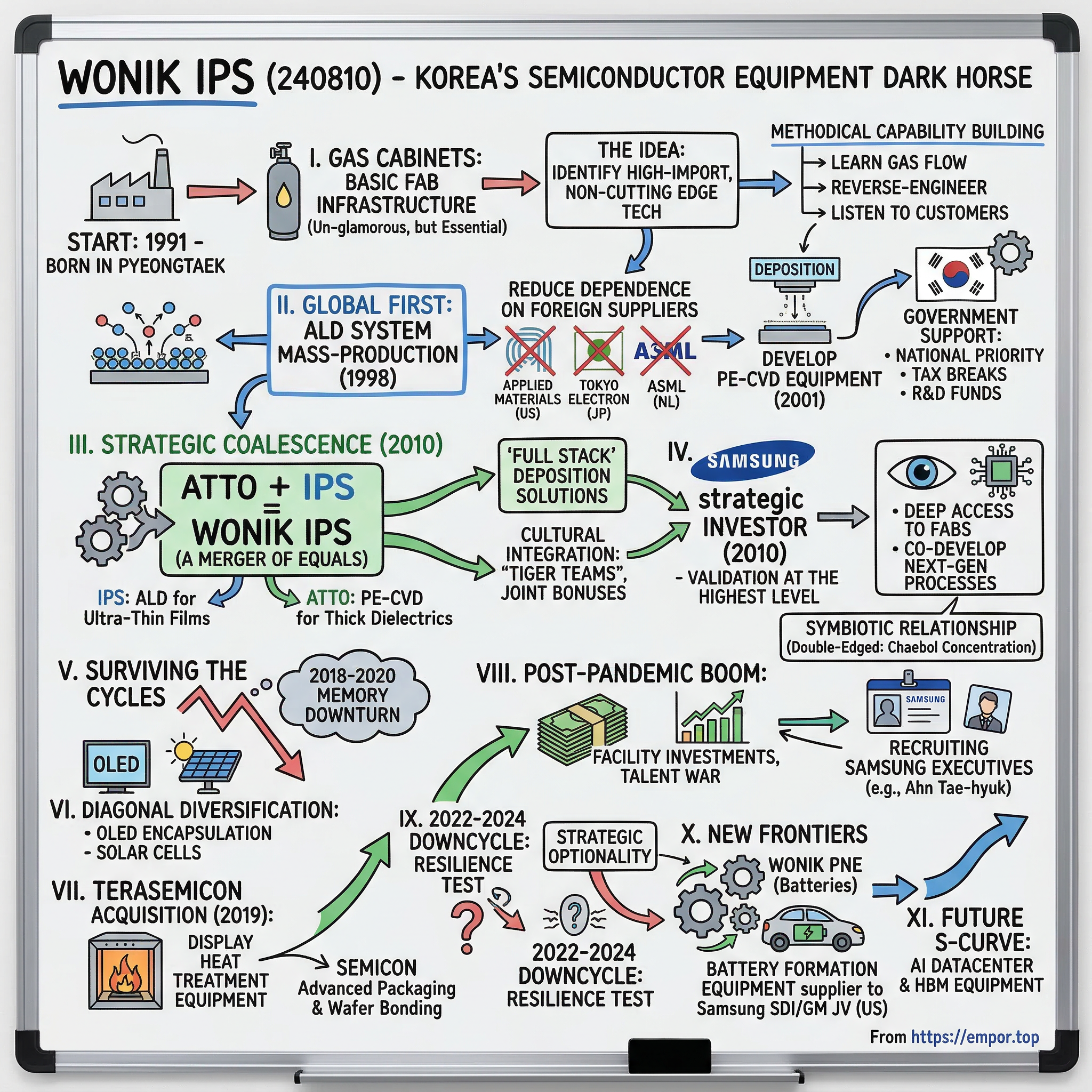
The rain was falling sideways in Pyeongtaek on a gray March morning in 2010. Inside a cramped conference room at IPS headquarters, executives were huddled around stacks of financial documents, their faces illuminated by the harsh fluorescent lights. After months of negotiations, they were about to sign the papers that would change everything—Samsung Electronics was converting 22 billion won of bonds, becoming a strategic investor in their company. For a local equipment maker that had spent two decades fighting to prove Korean technology could compete with Japanese and American giants, this was validation at the highest level.
How does a startup in Korea's industrial heartland, founded when the country's semiconductor industry was still importing virtually every piece of critical equipment, transform itself into a strategic partner to the world's largest memory chipmaker? This is the story of Wonik IPS—a company that bet everything on localization when "Korean equipment" was considered an oxymoron, survived multiple brutal semiconductor downturns that crushed its peers, and emerged as a rare example of successful industrial consolidation in Asia's most competitive tech ecosystem.
The puzzle pieces are fascinating: Founded in 1991 and headquartered in Pyeongtaek-Si, South Korea, Wonik IPS started when Korea's chip ambitions far exceeded its capabilities. Today, as of 30-Jun-2025, Wonik IPS has a trailing 12-month revenue of $603M, making it a mid-sized player by global standards but a critical piece of Korea's semiconductor sovereignty puzzle.
This episode traces three major themes that define not just Wonik IPS but the entire Korean equipment industry: the relentless pursuit of technological independence from foreign suppliers, the art of surviving cyclical devastation through strategic consolidation, and the delicate dance of being both supplier to and investment target of the mighty chaebols. We'll explore how a gas cabinet manufacturer became an ALD pioneer, why merging two successful companies at the market peak proved brilliant, and what it means to be Samsung's equipment partner in an industry where customer concentration can be both blessing and curse.
II. Origins & Korea's Semiconductor Ambitions
The year was 1991, and Korea's semiconductor industry was experiencing a profound identity crisis. Samsung and LG (then Lucky-Goldstar) were ramping up memory production, but walk into any Korean fab and you'd find a United Nations of equipment: Applied Materials from America, Tokyo Electron from Japan, ASML from the Netherlands. The dependency was complete, expensive, and strategically dangerous. Every equipment purchase meant technology fees flowing overseas, lengthy service waits for repairs, and the constant fear that geopolitical tensions could cut off supply chains overnight.
Into this environment stepped the founders of what would become Wonik IPS. Since its foundation in 1991, WONIK IPS has been greatly contributed to Korea's semiconductor equipment industry. They didn't start with grand ambitions of competing with Applied Materials—that would have been laughable. Instead, they identified the most basic, unglamorous piece of fab infrastructure: gas cabinets, the systems that safely deliver process gases to semiconductor tools. It wasn't cutting-edge technology, but it was essential, expensive to import, and something Korean engineers could realistically build.
Starting with gas cabinet production in 1991, the company succeeded in producing and commercializing atomic layer deposition (ALD) equipment, which is crucial in semiconductor production in 1996. This five-year journey from gas cabinets to ALD wasn't luck—it was methodical capability building. Each gas cabinet installation gave Wonik engineers precious access to Samsung and LG fabs. They studied how gases flowed, how contamination occurred, how temperature and pressure affected deposition. They recruited engineers who had trained abroad, reverse-engineered competitor products, and most crucially, listened obsessively to customer complaints about foreign equipment.
The early 1990s context made this possible. Korea's government, still flush with pride from hosting the 1988 Olympics, had declared semiconductor independence a national priority. The Ministry of Trade and Industry offered tax breaks for equipment purchases from domestic suppliers, funded R&D consortiums between chipmakers and equipment companies, and essentially forced Samsung and LG to give local suppliers a chance. It was industrial policy at its most aggressive—pick winners, protect them, and push them to compete globally.
But government support only opens doors; companies still had to deliver. Wonik's early clients were brutal in their feedback. One Samsung engineer famously told them their first ALD prototype "wouldn't be fit for a university lab, let alone our fab." Yet they persisted, iteration after iteration, because the alternative—permanent technological dependence—was unacceptable. In 2001, the company developed and started to supply PE-CVD equipment, contributing to reducing production cost for the Korean semiconductor industry that used to entirely rely on import.
III. The ALD Breakthrough & Early Growth
The breakthrough moment came in 1996 when Wonik successfully deposited its first uniform thin film using their homegrown ALD system. But the real milestone arrived two years later: Wonik IPS succeeded in mass-producing ALD systems in 1998 for the first time in the world. This wasn't just first in Korea—this was a global first for mass production of these systems, beating established players who had been too focused on CVD technology to see ALD's potential for ultra-thin films.
The technology itself was elegant in its precision. While Chemical Vapor Deposition (CVD) floods a wafer with reactive gases, ALD works through sequential, self-limiting reactions—like painting one molecular layer at a time. For the sub-100nm devices Samsung was planning, this atomic-level control would prove essential. Wonik's engineers had stumbled onto the right technology at exactly the right moment in Moore's Law progression.
Breaking the Japanese/US equipment monopoly required more than just technical capability. Wonik had to overcome what industry insiders called the "nobody ever got fired for buying Applied Materials" mentality. Their strategy was clever: target the process steps where import costs were highest and service requirements most demanding. ALD for high-k gate dielectrics became their wedge. When a Tokyo Electron system went down, it could take days for a technician to fly from Japan. Wonik could have someone on-site in hours.
Based on world-class technology, the company supplies to Korean companies such as Samsung, SK Hynix, and LG Philips, as well as global semiconductor and equipment companies around the world. Building credibility with Samsung and SK Hynix wasn't a single breakthrough but thousands of incremental improvements. Particle counts had to drop from hundreds to dozens to single digits. Throughput had to increase from 20 wafers per hour to 60. Mean time between failures had to extend from days to months.
The R&D investments were crushing for a company of Wonik's size. In the late 1990s, they were spending 15-20% of revenue on R&D, compared to 3-5% for mature equipment makers. They hired PhDs from Seoul National University and KAIST, sent engineers to conferences at SEMICON and IEDM, and created what they called "shadow teams" that would follow each customer's technology roadmap two nodes ahead. When Samsung started planning 90nm DRAM, Wonik was already testing films for 65nm.
We reinvented ourselves as a general machinery manufacturer as we diversified our portfolio to include not only semiconductor systems but also dry etchers in display and organic and inorganic deposition in PE-CVD and solar cells. This diversification wasn't just opportunistic—it was strategic hedging against semiconductor cycles that could destroy single-product companies overnight.
IV. The Strategic Merger: ATTO + IPS = Wonik IPS
By 2010, Korea's semiconductor equipment landscape had become a graveyard of ambitious failures. Dozens of companies had tried to scale up during the 2007-2008 boom, only to be crushed when the financial crisis triggered the worst semiconductor downturn in decades. IPS and ATTO were among the few survivors, but survival alone wouldn't be enough for what was coming. The industry was consolidating globally—Applied Materials attempting to buy Tokyo Electron, Lam Research acquiring Novellus. Scale was becoming destiny.
The numbers told the story: IPS reached KRW 100 billion in annual sales while ATTO Reached KRW 100 billion in PE-CVD sales. Two successful companies, each with nine-figure revenues, complementary technologies, and overlapping customer bases. The merger logic was compelling on paper, but in Korea's hierarchical business culture, mergers of equals almost never worked. Someone had to be the acquirer, someone the acquired, and face would be lost.
In December 2010, ATTO and IPS merged, creating an entity with combined revenues exceeding 200 billion won—suddenly large enough to matter on Samsung's supplier scorecard. The integration challenges were immense. ATTO's engineers, proud of their PECVD leadership, initially resisted reporting to IPS management. IPS's sales team, with deeper Samsung relationships, had to incorporate ATTO's SK Hynix connections without triggering customer conflicts.
The complementary technologies proved the merger's genius. IPS brought atomic layer deposition for ultra-thin films; ATTO contributed plasma-enhanced CVD for thick dielectrics. Together, they could offer what they called "full stack" deposition solutions—every layer from substrate to final passivation. When a customer needed to deposit a complex film stack with five different materials, they no longer had to coordinate between multiple vendors. One throat to choke, as procurement managers liked to say.
The cultural integration took years. They instituted "Tiger Teams" mixing engineers from both companies, forced joint customer visits, and most cleverly, tied bonuses to combined company performance rather than legacy division results. The new Wonik IPS that emerged wasn't just bigger—it was fundamentally more capable, able to tackle system-level problems that neither company could have solved alone.
V. The Samsung Partnership & Strategic Investment
In March 2010, IPS issued the corporate bond (CB) of KRW 22 billion assumed by Samsung Electronics. The announcement sent shockwaves through Korea's semiconductor equipment industry. Samsung, notorious for keeping suppliers at arm's length, was taking an equity stake in a domestic equipment maker. For Wonik IPS, it was like being knighted by the king.
But Samsung's investment was about more than money—it was about technology co-development in an era when equipment and process were becoming inseparable. As devices shrank below 20nm, you couldn't just buy off-the-shelf equipment and expect it to work. Process recipes had to be developed jointly, with equipment makers essentially becoming extensions of chipmakers' R&D teams. Samsung needed partners who could keep their secrets and iterate at Samsung speed.
The symbiotic relationship manifested in subtle but crucial ways. Wonik engineers received badges allowing them deep access to Samsung fabs—not just the production floor but the R&D pilot lines where next-generation processes were developed. Samsung's engineers, in turn, would spend weeks at Wonik's facilities, teaching them not just what specifications to hit but why those specs mattered for device performance. It was knowledge transfer at the atomic level.
Wonik IPS was awarded with the 2nd Semiconductor Day's Prime Minister Award, government recognition that validated their transformation from local supplier to national champion. The award ceremony photos—Wonik executives flanked by Samsung procurement chiefs and government ministers—captured Korea Inc. at its most coordinated.
Yet the Samsung relationship was double-edged. Other customers worried about IP leakage, wondering if their process secrets might flow to Samsung through shared equipment platforms. International customers were especially skeptical. Wonik had to create "clean room" engineering teams that were contractually walled off from Samsung projects, adding complexity and cost to their operations. The price of having a chaebol anchor: everything became political.
VI. Surviving the Cycles: 2018-2020 Memory Downturn
The memory market's 2018 collapse arrived with shocking suddenness. One quarter, Samsung and SK Hynix were printing money with DRAM prices at historic highs. The next quarter, inventory was piling up in warehouses as smartphone sales stalled and cryptocurrency mining crashed. Following record revenues in both 2017 and 2018, 2019 was a historical down cycle for both DRAM and NAND as demand grew stagnant.
For Wonik IPS, the downturn's timing was particularly cruel. They had just completed a major capacity expansion, hiring hundreds of engineers and building new cleanroom facilities to support what everyone assumed would be continued memory expansion. Instead, DRAM revenue declined 37.5% due to an oversupply that revealed the industry's persistent inability to match supply with demand.
The memory downcycle's anatomy was textbook in its devastation. Year-over-year memory sales growth in December 2018 registered -3.1 percent, the first negative growth rate of this cycle. But what made this cycle different was its origin—not a macroeconomic shock but technology transition delays. The shift to EUV lithography was taking longer than expected, 5G rollout was delayed, and AI hadn't yet emerged as the demand driver it would become.
Wonik's response revealed hard-learned lessons from previous cycles. Rather than mass layoffs, they shifted engineers to R&D projects that had been backburnered during the boom. They accelerated display equipment development, betting correctly that OLED adoption would continue despite smartphone weakness. Most presciently, they maintained their service operations at full strength, knowing that when customers cut capex, they become obsessed with extending existing equipment life.
The numbers from this period capture the brutality: memory equipment orders dropping 60%, lead times collapsing from 12 months to 12 weeks, and pricing pressure that forced 15-20% discounts just to keep production lines running. Yet Wonik survived where others failed through what executives called "diagonal diversification"—not abandoning semiconductor equipment but expanding into adjacent applications like solar cell deposition and display heat treatment that used similar core technologies but followed different demand cycles.
VII. The Tera Semicon Acquisition & Scale Play
Wonik IPS's most recent deal was a Merger/Acquisition with WONIK Tera Semicon. The deal was made on 01-Feb-2019. While the memory market was cratering around them, Wonik IPS made a contrarian bet, acquiring Wonik Tera Semicon for approximately KRW 150 billion. To outside observers, buying a display equipment company during a semiconductor downturn seemed like doubling down on cyclical misery.
Wonik IPS has strengths in the semiconductor equipment business while Wonik Terasemicon has strengths in the display heat treatment equipment business. The strategic logic was about technology convergence. As semiconductor companies pushed into advanced packaging and heterogeneous integration, they needed furnace technology for wafer bonding and annealing—exactly what Tera Semicon had developed for display manufacturing. The same thermal processing that crystallized silicon for LCD backplanes could enable next-generation 3D chip architectures.
Building critical mass across multiple verticals transformed Wonik's customer conversations. Instead of competing for individual tool purchases, they could propose integrated solutions. A memory customer needing both deposition and thermal processing could get both from Wonik, with guaranteed process compatibility and single-vendor accountability. The acquisition math was simple: 1+1=3 in customer value proposition.
Industry insiders predicted that this merger would lead to the birth of a huge South Korean equipment company that makes more than 1 trillion KRW in annual sales. The integration proved smoother than the earlier ATTO merger, perhaps because the memory downturn created urgency that overrode territorial disputes. When survival is at stake, engineers stop caring about whose technology gets top billing.
The furnace technology addition enabled vertical integration that competitors couldn't match. While Applied Materials had to partner with other companies for thermal processing, Wonik could optimize entire process flows internally. This proved especially valuable in emerging applications like silicon carbide processing for power semiconductors, where deposition and annealing steps had to be precisely coordinated.
VIII. Post-Pandemic Boom & Samsung Brain Drain
The pandemic's semiconductor supercycle caught everyone by surprise. What started as supply chain disruption morphed into unprecedented demand as work-from-home drove PC sales, streaming exploded, and governments printed money that flowed into electronics purchases. For Wonik IPS, orders that had evaporated in 2019 suddenly returned with vengeance.
Wonik IPS recorded 1.2323 trillion won in sales and 164.1 billion won in operating profit last year. As equipment supply increased due to facility investments worth 50 trillion won by Samsung Electronics and SK Hynix last year, sales and operating profit increased 13% and 17%, respectively, year-on-year. The numbers were staggering, but what really changed was Wonik's ability to attract talent from Samsung itself.
The talent war represented a seismic shift in Korea's rigid corporate hierarchy. Wonik Group is increasingly recruiting executives from Samsung to expand its business. Last year, Wonik IPS and Wonik PNE, major affiliates of semiconductors and batteries, also acquired personnel from Samsung. For decades, the career path was one-way: join a chaebol out of university, stay until retirement. Now Samsung executives were jumping to suppliers, bringing not just technical expertise but invaluable knowledge of how Samsung actually made purchasing decisions.
The company named Ahn Tae-hyuk as head and president of its semiconductor research lab. Ahn was last the executive vice president at Samsung SDI, where he oversaw their small and electric vehicle battery businesses from 2017 to 2021. Ahn's appointment was particularly symbolic—a Samsung lifer with three decades of experience choosing to lead R&D at a supplier. His network alone was worth millions in future orders.
Director Ahn worked for Samsung Semiconductor for more than 30 years and, as the head of the System LSI Manufacturing Center, was in charge of developing mobile application processors as well as memory semiconductors. This wasn't just hiring for expertise but for translation capability—someone who could speak both Samsung's language and explain to Wonik engineers what Samsung really needed versus what their RFQs claimed they wanted.
IX. The 2022-2024 Downcycle & Resilience Test
The semiconductor down cycle that started in the second half of 2022 is still showing no signs of recovery. After the pandemic boom, the hangover arrived with predictable brutality. Consumers who had upgraded everything during lockdowns stopped buying, enterprises realized they'd over-ordered, and inflation crushed discretionary spending. The memory market, as always, crashed hardest.
The memory market fared worse, at $19.3 billion in the first quarter of 2023, just 44 per cent of the first quarter of 2022 ($43.6 billion). For equipment makers like Wonik, the impact was delayed but devastating. Chip makers first run down equipment inventory, then cancel orders, then demand pricing concessions on committed purchases. The playbook never changes, only the magnitude of pain.
Yet this downcycle felt different—less about oversupply than demand destruction. Bit demand, or the total memory capacity being bought, is weak at the moment. Typically, bit demand remains the same while the price fluctuates, but the memory makers are being hit by a double whammy right now. Previous downturns saw prices collapse but volumes remain stable. This time, nobody wanted memory at any price.
As of 30-Jun-2025, Wonik IPS has a trailing 12-month revenue of $603M, demonstrating resilience but clear pressure from the cycle. The stock market's verdict has been harsh but not catastrophic—the company remains valued at nearly $1 billion despite the downturn, suggesting investors believe in the eventual recovery.
Current positioning reveals strategic evolution beyond pure cycle riding. Wonik has maintained R&D spending above 15% of revenues even as profits evaporated, betting that the next upturn will reward those who invested through the downturn. They've also pushed harder into China, accepting geopolitical risk for diversification away from Samsung and SK Hynix concentration.
X. New Frontiers: Display, Battery, and Beyond
The non-semiconductor expansion strategy emerged from brutal cycle experience—when memory capex drops 50%, you need other revenue sources or you die. Wonik's approach was strategic adjacency: find markets that use similar manufacturing technologies but follow different investment cycles.
With the successful acquisition of PNE Solutions and NS, Wonik PNE has now become a company that deals with battery processes. Although the M&A for the display equipment business between SEMES has fallen through, Wonik concentrated on acquiring the battery sector and added a battery equipment business. The battery equipment push proved particularly prescient as electric vehicle adoption accelerated and every automaker scrambled to secure battery supply chains.
Display equipment offered another diversification avenue. OLED adoption for smartphones was mature, but emerging applications in automotive, AR/VR, and foldable devices created new equipment opportunities. They are developing a PECVD equipment, which is used in the encapsulation process (a key part of OLED production). This equipment is optimized for the TFE (Thin Film Encapsulation) process. The technology synergies were obvious—thin film deposition is thin film deposition, whether for semiconductors or displays.
Wonik PNE has been selected as the supplier of formation equipment to the battery joint venture between Samsung SDI and General Motors, which is building a factory in New Carlisle, Indiana in the US. Formation equipment are used in the final stages of battery assembly to charge and discharge current to the batteries, making them active. Samsung SDI and General Motors' joint venture is planning to secure a production capacity of 36GWh per year, so Wonik PNE is expected to win orders worth over 100 billion won.
Building optionality for the next cycle required patient capital and strategic courage. While competitors retreated to core markets during downturns, Wonik kept investing in emerging applications. Solar cell equipment had failed before but might succeed with new perovskite technologies. Power semiconductor equipment for silicon carbide and gallium nitride served smaller markets but with better margins and less Chinese competition.
XI. Playbook: Business & Investing Lessons
Lesson 1: The power of localization in strategic industries. Wonik's success demonstrates that in industries deemed strategically critical, technical parity can be enough if you offer superior service, faster iteration, and government support. The company didn't need to be better than Applied Materials—being 90% as good with 50% faster response time was enough to win Korean business.
Lesson 2: Consolidation as survival strategy in cyclical markets. The ATTO and Tera Semicon mergers, both executed at cycle peaks when valuations were high, seemed poorly timed. Yet they provided the scale and technical breadth to survive subsequent downturns. In equipment markets, you consolidate when you can, not when you must.
Lesson 3: Strategic investor relationships in Asian markets. Samsung's investment provided more than capital—it offered validation, technology access, and guaranteed order flow. The cost in independence was worth the benefits in credibility. For equipment companies in chaebol-dominated economies, strategic alignment with a major customer becomes existential.
Lesson 4: Talent acquisition from giants as growth accelerator. Hiring Samsung executives wasn't just about expertise but about understanding how decisions really get made in Korean conglomerates. Every ex-Samsung VP brought a Rolodex worth millions in potential orders and insights into procurement processes that no consultant could provide.
Lesson 5: Multi-vertical diversification in equipment markets. Pure-play semiconductor equipment companies face extreme cyclicality. Wonik's expansion into displays, batteries, and solar—all using similar core deposition and thermal technologies—provided cycle insurance without abandoning core competencies.
The Korea Inc. playbook emerged clearly: government support to overcome initial technology gaps, chaebol partnerships for scale and validation, aggressive M&A during upturns to build critical mass, and relentless focus on the next technology node. It's industrial policy as venture capital, with the state and conglomerates acting as patient capital providers for strategic industries.
XII. Bear vs. Bull Case Analysis
Bear Case:
The extreme customer concentration remains Wonik's Achilles heel. With Samsung and SK Hynix representing approximately 70% of revenues, Wonik is essentially a leveraged bet on Korean memory production. If Samsung ever decided to shift equipment purchases to global suppliers for technology or political reasons, Wonik would face existential crisis overnight.
Cyclical exposure to memory markets creates violent earnings swings that make planning impossible. When memory capex can drop 50% in a single year, maintaining R&D spending and talent becomes a constant struggle. The current downcycle, potentially extending through 2025, tests whether Wonik has truly learned from past crashes or will repeat the same mistakes.
Competition from global giants remains overwhelming. Applied Materials generates more revenue in a quarter than Wonik does in a year. Tokyo Electron's R&D budget exceeds Wonik's total revenues. In any technology race, Wonik starts from behind and must run faster just to keep pace. As semiconductors approach atomic scales, the technology barriers favor incumbents with deeper pockets.
Geopolitical risks loom larger than ever. U.S. restrictions on equipment sales to China, potential technology controls on Korea, and the general fracturing of global supply chains all threaten Wonik's growth ambitions. Being caught between U.S. technology restrictions and Chinese market opportunities creates no-win scenarios.
Bull Case:
Wonik's critical position in the Korean semiconductor ecosystem provides a competitive moat that global competitors can't breach. Cultural alignment, language advantages, and physical proximity create switching costs that protect incumbent positions. As long as Korea remains a memory superpower, Wonik has guaranteed relevance.
Expansion into next-generation technologies positions Wonik for secular growth beyond cycles. EUV layers require new deposition techniques where historical advantages matter less. High-bandwidth memory for AI applications needs novel equipment approaches. Battery equipment represents a completely new growth vector as electric vehicle adoption accelerates globally.
Battery and display diversification genuinely reduces cycle dependency. While semiconductor equipment orders collapsed in 2023, battery equipment orders surged as automakers built gigafactories. Display equipment for automotive and AR/VR applications follows consumer product cycles, not semiconductor investment patterns.
Valuation discount to global peers despite similar technology creates opportunity. Trading at significant discounts to companies like Lam Research or Tokyo Electron despite comparable gross margins suggests market skepticism that could reverse with continued execution. If Wonik can demonstrate consistent performance through a full cycle, multiple expansion alone could drive significant returns.
XIII. Epilogue & "If We Were CEOs"
Standing in Wonik's Pyeongtaek headquarters today, you see a company at an inflection point. The gleaming cleanrooms and advanced R&D labs suggest global ambitions, yet the customer concentration and cycle dependence reveal persistent vulnerabilities. Can a regional champion become a global leader, or will Wonik forever remain Korea's best-kept equipment secret?
The path to Top 10 global equipment status requires breaking the Korea dependency. International expansion can't just mean selling to Samsung's overseas fabs—it means winning at TSMC, Intel, and eventually Chinese nationals. This requires not just technical capability but cultural transformation, from Korean-first to globally native. Every successful equipment company eventually faces this transition; most fail.
M&A opportunities in complementary technologies could accelerate growth beyond organic expansion. Acquiring metrology capabilities, software competencies, or service operations in other geographies could transform Wonik from product vendor to solution provider. The challenge: finding targets that are both affordable and strategically valuable in an industry where everyone knows everyone's technology.
The AI datacenter opportunity and HBM equipment needs represent the next S-curve of growth. High-bandwidth memory requires different deposition approaches, tighter process control, and system-level optimization that favors integrated suppliers. If Wonik can position itself as the HBM equipment specialist while globals focus on logic, a profitable niche awaits.
If we were CEOs, the strategic priorities would be clear: diversify customer concentration through aggressive international expansion, build software and service capabilities that create recurring revenues, and position for the AI infrastructure buildout that will drive the next semiconductor supercycle. The window is narrow—perhaps 18-24 months before the next upturn solidifies competitive positions for the next decade.
Final reflection: Wonik IPS embodies both the triumph and tragedy of Korea's industrial model. The triumph: building world-class technology from nothing through sheer determination. The tragedy: remaining perpetually dependent on a few customers in a brutally cyclical industry. Whether Wonik transcends these constraints to become a truly global leader will determine not just one company's fate but whether Korea's equipment industry can finally step out from the shadow of its chaebol customers.
XIV. Outro & Resources
The Wonik IPS story offers profound lessons for understanding industrial policy, technology catch-up strategies, and the realities of competing in capital-intensive industries. Key sources that informed this analysis include company filings with the Korea Exchange, SEMI's equipment market reports tracking the brutal cycles, and the broader context of Korean semiconductor history from government white papers and industry association reports.
For those seeking deeper understanding, "Samsung Rising" by Geoffrey Cain provides essential context on Korea's semiconductor ambitions, while "The Chip War" by Chris Miller explains the global dynamics that created opportunities for companies like Wonik. The Korean Development Institute's studies on industrial policy offer frameworks for understanding how government support enabled domestic equipment makers to challenge global incumbents.
The semiconductor equipment industry stands at another inflection point as AI drives demand, geopolitical tensions reshape supply chains, and new technologies like quantum computing threaten to obsolete existing paradigms. Companies that survive the current downturn while investing in next-generation capabilities will define the industry's next chapter. Whether Wonik IPS becomes a protagonist or footnote in that story remains unwritten, but their journey from gas cabinet supplier to Samsung partner demonstrates that with enough persistence, even the most ambitious industrial transformations are possible.
 RSS Feed
 Spotify
 Apple Podcasts
 Amazon Music
 Audible
 YouTube