Kinik Company: From Taiwanese Grinding Wheels to Global Semiconductor Essential
I. Introduction & Cold Open
Picture this scene: Deep in the heart of Taiwan's semiconductor ecosystem, thousands of tiny diamonds—each precisely positioned in a metal grid—polish silicon wafers to atomic-level smoothness. Without this critical step, the chips powering everything from smartphones to AI data centers would fail. The company behind these diamond tools? Not ASML, not Applied Materials, but a 70-year-old grinding wheel manufacturer from a pottery village in Taiwan.
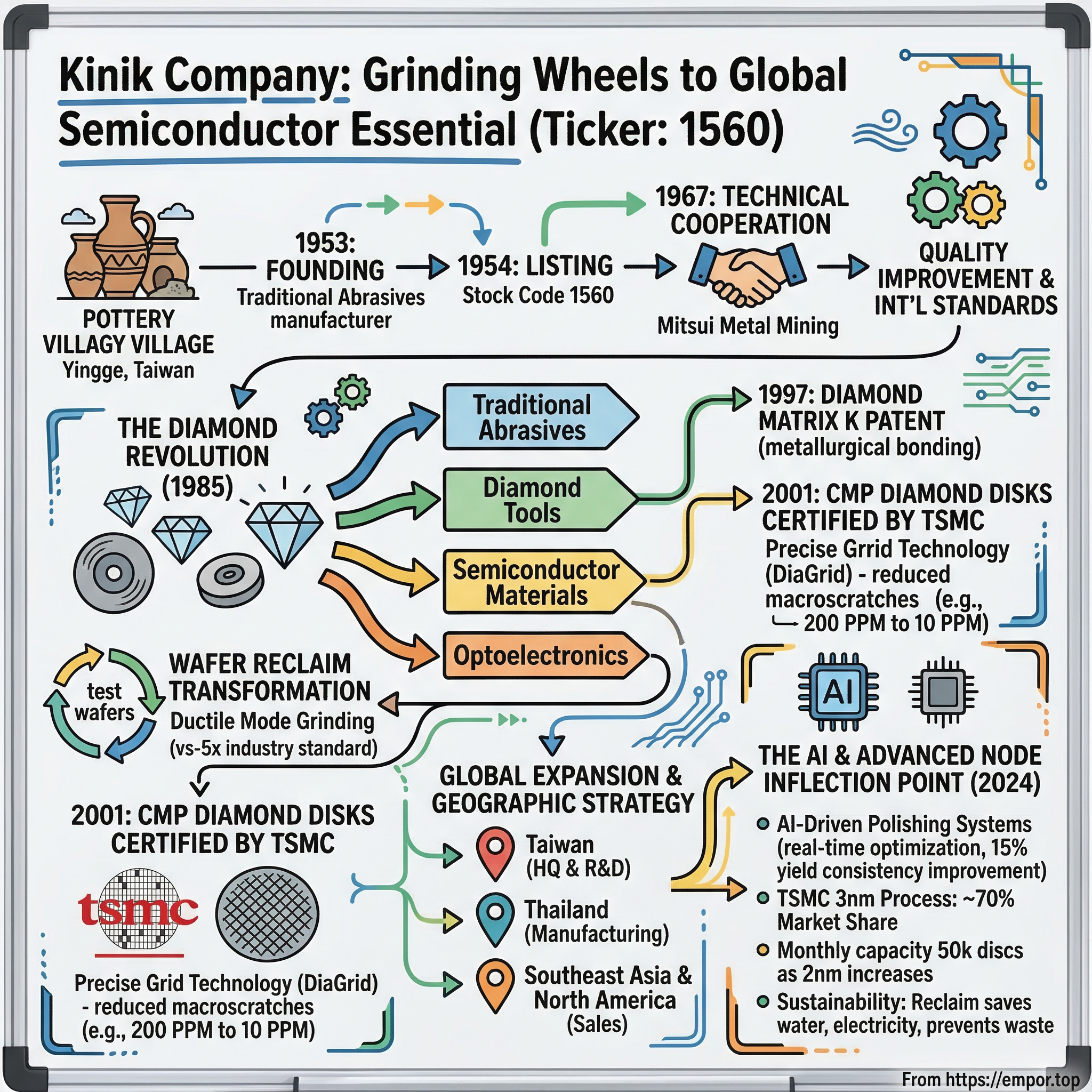
Kinik Company was founded in 1953 and is headquartered in New Taipei City, Taiwan. What began as a traditional abrasives manufacturer in Taiwan's post-war industrial awakening has transformed into an indispensable player in the global semiconductor supply chain. According to market reports, Kinik holds a 70% market share for TSMC's 3-nanometer process technology. This is the story of how a grinding wheel company from Yingge—Taiwan's famous ceramics center—became the hidden champion enabling Moore's Law.
The transformation from mechanical grinding wheels to semiconductor-grade diamond tools represents one of the most successful pivots in Taiwan's industrial history. Today, Kinik operates across four distinct business units—Traditional Abrasives, Diamond Tools, Semiconductor Materials, and Optoelectronics—serving over 8,000 customers worldwide with more than 100,000 product specifications. The current market capitalization of Kinik is $1.58B.
This episode explores how geographic proximity, technical partnerships, and perfectly timed strategic pivots created a company that most people have never heard of, yet touches nearly every semiconductor manufactured today.
II. Origins & The Pottery Village Beginning
The narrow streets of Yingge Township wind through centuries of ceramic tradition. It is famous for the production of porcelain and an abundance of art studios and shops. Here, where clay has been shaped into pottery since the Qing Dynasty, a different kind of precision manufacturing was about to emerge.
Kinik Company is a specialized grinding wheel manufacturer with more than 50 years history, which located in the famous place of ceramics and pottery in Taiwan - Yingee Township. The company emerged during Taiwan's post-war industrial reconstruction, when the island was transitioning from agricultural economy to manufacturing powerhouse. In 1954, just one year after founding, the stock was officially listed on January 31 with stock code 1560—a remarkably early public listing that reflected both ambition and the capital needs of industrial expansion.
The breakthrough came through international collaboration. In 1967 Kinik Company cooperated with Mitsui Metal Mining Co., Ltd. in technical aspect, improving product quality. This wasn't just a licensing deal—it was a comprehensive technology transfer that brought Japanese manufacturing precision to Taiwan. The relationship between the two companies dates back to the 1960s, when they began technical collaboration. The partnership provided Kinik with access to advanced sintering techniques, quality control methodologies, and most importantly, credibility with international customers who trusted Japanese industrial standards.
By 1984, the company had scaled dramatically. Production capacity reached 250 metric tons monthly, ranking among the top five grinding wheel factories in Asian free regions. The location in Yingge wasn't accidental—the township's expertise in high-temperature kilns and ceramic processing provided both skilled workers and technical knowledge directly applicable to abrasive manufacturing. Workers who understood how to control furnace temperatures for pottery glazing could adapt those skills to sintering grinding wheels.
The company's evolution reflected Taiwan's broader industrial strategy. While Korean chaebols pursued vertical integration and Japanese keiretsu maintained closed supplier networks, Taiwanese companies like Kinik specialized deeply in specific components, becoming indispensable nodes in global supply chains. This pattern would prove prescient as the semiconductor industry emerged.
III. The Diamond Revolution & Business Unit Strategy
The year 1985 marked a fundamental shift in Kinik's technological trajectory. BD wheel manufacturing Department was established in 1985 for manufacturing porcelain and resin production of diamond and CBN grinding wheel. Diamond and cubic boron nitride (CBN) represented superabrasives—materials second only to diamond in hardness, capable of cutting and grinding materials that would destroy conventional wheels.
The technical challenges were immense. Unlike conventional abrasives where particles are distributed randomly through a binding matrix, diamond tools require precise control over particle placement, bonding strength, and protrusion height. Too much exposure and diamonds break off; too little and they don't cut effectively. The company spent years perfecting the metallurgical bonds that would hold diamonds firmly while allowing controlled wear.
In 1997 Diamond matrix K obtained the world patent. This wasn't just an incremental improvement—it represented a fundamental breakthrough in how diamonds could be brazed to metal substrates. The patent covered a novel bonding chemistry that created a metallurgical bond between diamond and substrate, dramatically improving retention and tool life. 2013-07-29 Assigned to KINIK COMPANY reassignment KINIK COMPANY AGREEMENTS AFFECTING INTEREST Assignors: SUNG, CHIEN-MIN, DR.
The strategic implications were profound. With this technology, Kinik could move beyond commodity grinding wheels into high-value precision tools. Applications ranged from cutting granite countertops to grinding tungsten carbide cutting tools, but the real opportunity lay elsewhere. As the company developed its diamond technology through the 1990s, Taiwan's semiconductor industry was simultaneously exploding. TSMC, founded in 1987, was pioneering the pure-play foundry model. UMC was expanding rapidly. The timing couldn't have been better.
By structuring itself into distinct business units—Traditional Abrasives, Diamond, and later Semiconductor Materials and Optoelectronics—Kinik created internal entrepreneurship. Each unit had its own P&L responsibility, could pursue distinct market opportunities, and critically, could share technologies across divisions. Diamond brazing techniques developed for stone cutting could be adapted for semiconductor applications. Precision grinding knowledge from traditional wheels informed wafer processing. This organizational structure would prove crucial as the company entered its next phase.
IV. The Semiconductor Pivot: CMP Diamond Disks
The conference room at TSMC's Hsinchu headquarters, 2001. Kinik's engineers presented a diamond disk that looked deceptively simple—a stainless steel substrate with thousands of diamonds embedded in precise patterns. But this disk would solve one of semiconductor manufacturing's most vexing challenges.
In 2001 polishing pad Finisher (diamond plate) used in the semiconductor CMP process was developed and certified by TSMC, being taken into mass production shipment. Chemical Mechanical Planarization (CMP) represents the intersection of chemistry and physics—using abrasive slurries and polishing pads to achieve atomic-level flatness on silicon wafers. As transistors shrank below 180 nanometers, even microscopic variations in surface height could cause manufacturing defects.
The problem with existing CMP pad conditioners was randomness. The production methods of the past tend to produce disks having diamonds that are clustered in groups, or unevenly spaced on the surface of the substrate. This uneven grouping causes some portions of the CMP pad to be overdressed which creates wear marks, while others are underdressed which creates glazing layers. Kinik's breakthrough came through their DiaGrid technology—diamonds arranged in precise grid patterns rather than random distribution.
A dresser that contains a diamond grid is much more efficient to dress the pad than conventional disks with randomly distributed grits. The benefits cascaded through the entire manufacturing process. On production scale, the diamond grid has significantly reduced the occurrence of macroscratches on wafers (e.g., from a typical rate of about 200 PPM to about 10 PPM for oxide CMP on Mirra machine). For semiconductor manufacturers operating on razor-thin margins where every percentage point of yield improvement translated to millions in revenue, these results were revolutionary.
TSMC's certification wasn't just a customer win—it was a seal of approval from the world's most advanced foundry. Kinik embeds thousands of diamonds in precise patterns on stainless steel disks. Other foundries took notice. Intel evaluated the technology. Samsung requested samples. The product that started as an experiment had become industry standard.
The technical moat deepened with each generation. As TSMC moved to smaller nodes, CMP requirements became more stringent. Flatness tolerances dropped from micrometers to nanometers. The number of CMP steps per wafer increased from 10 to over 30. Each change required co-development between Kinik and its customers, creating switching costs that made displacement nearly impossible. By 2005, Kinik had become so embedded in TSMC's process flows that changing suppliers would require requalifying entire production lines—a risk no operations manager would willingly take.
V. The Wafer Reclaim Transformation
The economics were compelling: a virgin 300mm silicon wafer cost $100-150. Reclaiming that same wafer—stripping, polishing, and cleaning it for reuse—cost $30-40. For semiconductor fabs running thousands of test wafers daily, the math was obvious. But execution proved anything but simple.
Kinik's entry into wafer reclaim came through acquisition and integration. In September, the company merged with affiliate Kinik Precision Grinding Corp. to form the Semiconductor Materials Business Unit. The timing aligned with a fundamental shift in semiconductor economics. As wafer sizes increased from 200mm to 300mm, the value of each wafer doubled while the reclaim cost increased only marginally. Suddenly, reclaiming wafers wasn't just about cost savings—it was about supply security.
The global Reclaim Wafer market was valued at USD 662.04 million in 2023 and is projected to reach USD 1.09 billion by 2030, reflecting a compound annual growth rate (CAGR) of 7.76% during the forecast period from 2024 to 2030. Kinik positioned itself as a technology leader, developing ductile mode grinding processes that replaced traditional lapping. This approach removed material atom by atom rather than through mechanical abrasion, preserving the crystal structure and enabling wafers to be reclaimed up to 10 times versus the industry standard of 3-5 times.
Leading global manufacturers in this market include RS Technologies, Kinik, Phoenix Silicon International, Hamada Rectech, Mimasu Semiconductor Industry, GST, Scientech, Pure Wafer, and TOPCO Scientific Co. LTD. In 2023, the top three companies collectively generated approximately 53.0% of the market's total revenue. While RS Technologies commanded the largest share at 33%, Kinik's technological differentiation allowed premium pricing.
The environmental angle provided unexpected leverage. As semiconductor companies faced increasing ESG scrutiny, wafer reclaim offered a compelling sustainability story. Each reclaimed wafer saved 1,500 liters of ultrapure water, 20 kWh of electricity, and prevented 2.3 kg of chemical waste. For companies like Apple pressuring suppliers on environmental metrics, Kinik's reclaim services became part of the solution.
The business model proved remarkably resilient. During semiconductor downturns when fabs reduced capital spending, they increased wafer reclaim to cut costs. During upturns when wafer supply tightened, reclaim provided additional capacity. This countercyclical dynamic smoothed revenue volatility, providing ballast to Kinik's more cyclical equipment sales.
VI. The Optoelectronics Adventure & Molded Lens Partnership
The year 2005 brought an unexpected opportunity. Taiwan's government launched the "Two-Trillion, Two-Star Project"—an ambitious industrial policy targeting semiconductors, flat panel displays, digital content, and biotechnology. For Kinik, this signaled a chance to leverage its precision manufacturing capabilities in a new domain: optical components.
In November, the company launched production of aspheric molded optical glass lenses. These weren't ordinary lenses—aspheric profiles required nanometer-precision molding that pushed the boundaries of glass forming technology. Traditional lens grinding could achieve the shapes but at prohibitive costs. Molding offered the possibility of mass production at price points suitable for consumer electronics.
The partnership strategy proved crucial. The Time of Establish:March 27th, 2018 Chairman:TOMOYUKI TAGUCHI Capital:300 Million (NTD) Nihon Yamamura Glass Co., Ltd. (NYG) 70% KINIK Company (KINIK) 30% Business Items:Manufacture and sale of optical molding glass lens Nihon Yamamura brought 100 years of glass expertise; Kinik contributed precision mold-making capabilities developed through its grinding wheel business. We manufacture and sell aspheric lens products mainly for the optical communication field where expansion is expected in the future. Our core technology is fusion by each company's advantage that optical design, ultra-precision metal processing, surface modification, press processing, and hermetic sealing from KINIK, and material design, glass processing, various items held by NYG group.
The initial target market seemed perfect: smartphone cameras transitioning from single to multiple lenses, digital cameras demanding higher quality optics, and emerging applications in optical communications. The company developed molds capable of maintaining surface profiles within 0.1 micrometers across thousands of pressing cycles. Products ranged from 2mm smartphone camera lenses to 30mm projector optics.
Yet the venture ultimately proved challenging. Chinese competitors, backed by government subsidies, flooded the market with lower-cost alternatives. Smartphone manufacturers consolidated lens suppliers, favoring larger players with broader component portfolios. By 2019, The optical molding glass lens business was transferred from KINIK to YKO in 2019. The joint venture structure remained, but Kinik's direct involvement diminished.
The optoelectronics experience taught valuable lessons. Technical excellence alone wasn't sufficient in consumer electronics where cost, scale, and customer relationships determined success. The company's subsequent strategic decisions would reflect this learning, focusing on markets where technical differentiation commanded premium pricing and customer relationships created lasting moats.
VII. Global Expansion & Geographic Strategy
The morning of July 1st marked a new chapter. 225 Moo 7, Khok Pip, Simahosot, Prachinburi 25190 Thailand [email protected] Kinik's new Thai subsidiary began operations, but this wasn't just about low-cost manufacturing. The location—strategically positioned between automotive clusters and emerging electronics assembly operations—represented a calculated bet on supply chain diversification.
Based on the historical data available with Volza, the company has exported 2,294 shipments to 8 buyers. The primary markets for these exports were Indonesia, the Vietnam, and Philippines. The Southeast Asian expansion served multiple strategic objectives. First, it provided natural hedging against Taiwan's geopolitical risks. Second, it offered proximity to fast-growing markets where infrastructure development drove demand for cutting tools and industrial abrasives. Third, and perhaps most importantly, it created redundancy in the supply chain that global customers increasingly demanded.
The expansion wasn't without challenges. Managing quality across multiple sites required standardizing processes that had evolved organically over decades in Taiwan. The company implemented digital twin manufacturing—replicating exact process parameters from Taiwan facilities to ensure product consistency. Engineers from Yingge spent months in Thailand training local staff not just on procedures but on the underlying metallurgy and chemistry.
The US-China trade tensions beginning in 2018 validated the strategy. As semiconductor companies scrambled to diversify supply chains, Kinik could offer production from both Taiwan and Thailand. When customers requested "non-China" sourcing attestations, Kinik could comply without disrupting operations. MGT has a strong sales network in Japan and Southeast Asia, while KINIK has a presence in Taiwan, China, and North America, creating a global market complementarity. Incorporating KINIK's semiconductor expertise into MGT's automotive-focused business will drive expansion into new industries.
Headquarters, meanwhile, relocated within Taiwan—from the original Yingge site to a modern campus in the same district. The move was symbolic and practical. Symbolic in maintaining roots in the pottery township that birthed the company. Practical in providing expanded R&D facilities, clean rooms for semiconductor products, and proximity to both TSMC and Taiwan's extensive supplier ecosystem.
VIII. Financial Performance & Market Position
The numbers tell a story of consistent execution. In 2024, Kinik Company's revenue was 7.02 billion, an increase of 10.01% compared to the previous year's 6.38 billion. Earnings were 1.04 billion, an increase of 21.46%. But raw figures obscure the more interesting narrative: margin expansion through relentless movement up the value chain.
Consider the evolution of average selling prices. A traditional grinding wheel might sell for $5-10. A diamond wheel for industrial cutting: $50-100. A CMP pad conditioner for semiconductor manufacturing: $500-2,000. A full wafer reclaim service contract: $20,000-50,000 per month. Each step up required new capabilities, but also delivered exponentially higher margins.
reached NT$6.381 billion, representing a decline of 8% from 2022; the net profit after tax was NT$862 million, and the earnings per share after-tax were NT$5.91. The 2023 results reflected broader semiconductor industry headwinds as excess inventory from the pandemic boom worked through the system. Yet Kinik's profitability remained robust—13.5% net margins even in a down year demonstrated the resilience of the business model.
The balance sheet revealed conservative management. Debt-to-equity ratios below 0.3x, current ratios above 2.0x, and consistent free cash flow generation provided flexibility for both organic investment and opportunistic M&A. The company maintained dividend payments through cycles, understanding that many institutional investors in Taiwan prized stability over growth.
Geographic revenue mix had shifted dramatically. In 1990, 90% of sales were domestic. By 2024, international sales exceeded 60%, with particularly strong growth in Southeast Asia and North America. Customer concentration remained manageable—even TSMC, the largest customer, represented less than 15% of total revenue. This diversification protected against single-customer risk while maintaining deep strategic relationships.
The comparison with global peers proved instructive. While companies like Saint-Gobain operated at massive scale across multiple industries, Kinik's focused approach yielded superior returns on capital. The company consistently achieved ROE above 20%, well exceeding industry averages of 12-15%. The market recognized this execution—Kinik's P/E ratios consistently traded at premiums to both Taiwanese industrials and global abrasives manufacturers.
IX. The AI & Advanced Node Inflection Point
The future arrived with unusual clarity in 2024. Kinik Corporation Introduces AI-Driven Polishing Systems (2025): Kinik implemented artificial intelligence for real-time process optimization, improving wafer yield consistency by 15% and reducing reprocessing time. This wasn't just automation—it was intelligent adaptation, with machine learning algorithms adjusting polishing parameters in real-time based on wafer-by-wafer metrology data.
The AI transformation went deeper than press releases suggested. Inside Kinik's R&D labs, engineers trained neural networks on decades of process data—correlating diamond wear patterns with polishing outcomes, predicting pad degradation before it affected yields, optimizing slurry flow rates for different material stacks. The accumulated knowledge of master technicians was being encoded into algorithms.
The firm has increased its monthly production capacity to 50,000 discs, with sources adding that as TSMC increases 2-nanometer production, its disc revenue will mark sequential (quarter-over-quarter) growth. The numbers reflected fundamental changes in semiconductor manufacturing. As chipmakers pushed toward 2-nanometer nodes, the number of CMP steps per wafer increased from 30 to nearly 50. Each step required different consumables, different process parameters, different quality controls. Complexity became competitive advantage for companies like Kinik that could manage it.
The implications extended beyond traditional logic chips. Silicon Wafer Reclaim Market Size was valued at USD 0.89 Bn in 2024 and is expected to reach USD 3.37 Bn by 2032, at a CAGR of 18%. This explosive growth reflected new applications: silicon carbide wafers for electric vehicles requiring different reclaim processes than silicon, gallium nitride for 5G base stations demanding ultra-smooth surfaces, specialized substrates for quantum computing with zero-defect tolerance.
Sustainability emerged as an unexpected growth driver. Data centers powering AI applications consumed enormous amounts of electricity—by 2025, training a large language model required as much energy as 100 American homes use in a year. Chip manufacturers faced pressure to reduce environmental impact across the supply chain. Kinik's water recycling systems, chemical recovery processes, and wafer reclaim services positioned it as a solution provider rather than just a component supplier. The company's 2025 sustainability report showed 40% reduction in water usage per unit produced, 30% decrease in chemical waste, and carbon intensity improvements that exceeded Taiwan's industrial targets.
X. Playbook: Lessons from Kinik's Journey
Lesson 1: Timing Technology Transitions Kinik's history reads like a masterclass in technological timing. The shift from traditional to diamond abrasives (1985) preceded Taiwan's industrial upgrade. The semiconductor pivot (2001) aligned with the foundry model's ascendance. The wafer reclaim expansion (2010s) anticipated supply constraints. Each transition began before markets fully materialized but after technological feasibility was proven. The lesson: move when technology is ready, not when markets are obvious.
Lesson 2: The Power of Customer Certification Diamond disc obtained a certificate issued by TSMC. In B2B markets, marquee customer endorsements create cascading credibility. Kinik's TSMC certification opened doors at Samsung, Intel, and others. But certification went beyond marketing—it represented co-development, process integration, and genuine partnership. The deepest moats come from being embedded in customer success, not just selling to them.
Lesson 3: Geographic Advantage Taiwan's semiconductor ecosystem provided unique advantages: physical proximity to customers, shared talent pools, rapid iteration cycles. Engineers could visit TSMC in the morning, modify designs over lunch, and deliver prototypes by evening. This tight feedback loop—impossible with distant suppliers—accelerated innovation and deepened relationships. Geography still matters in the digital age.
Lesson 4: Diversification vs. Focus Debate Kinik's four business units might seem unfocused, but closer examination reveals strategic logic. Each unit shared core competencies in materials science and precision manufacturing while serving different markets. This portfolio approach provided resilience—when semiconductor markets declined, industrial abrasives compensated. Yet within each unit, the company maintained laser focus on specific applications where it could achieve leadership.
Lesson 5: Building Technical Capabilities Through Partnerships From Mitsui's 1967 technology transfer to Yamamura's optical joint venture to recent AI collaborations, Kinik consistently accessed external expertise while maintaining internal absorption capacity. The company didn't just license technology—it learned, adapted, and eventually surpassed teachers. True partnership requires humility to recognize gaps and confidence to bridge them.
Lesson 6: Riding Sustainability Tailwinds Environmental regulations transformed from compliance burden to competitive advantage. Kinik's wafer reclaim business exemplified this transition—what began as cost-saving service evolved into environmental imperative. Companies that reframe environmental challenges as business opportunities position themselves for regulatory tailwinds rather than headwinds.
XI. Power Analysis & Competitive Moats
Switching Costs: The semiconductor industry abhors change. Once Kinik's diamond disks are qualified in a fab's process flow, switching requires extensive requalification—typically 6-12 months and millions in validation costs. With yields measured in fractions of percentages and downtime costing $1 million per hour, operations managers refuse supplier changes unless absolutely necessary. These switching costs compound over time as process recipes accumulate around specific consumables.
Network Effects: Limited but present. Kinik benefits from Taiwan's semiconductor ecosystem density—shared knowledge flows, engineer mobility, and supplier interconnections. The company's participation in TSMC's supplier councils creates information advantages and early visibility into technology roadmaps. However, these effects remain regional rather than global.
Scale Economies: Manufacturing scale matters less than R&D scale in Kinik's markets. The company invests 3-5% of revenue in R&D, but more importantly, concentrates resources on specific technical challenges. This focused scale—deep rather than broad—enables breakthrough innovations like the diamond matrix patent that broader competitors missed.
Counter-positioning: Against virgin wafer producers, Kinik's reclaim business represents true counter-positioning. Virgin wafer makers cannot embrace reclaim without cannibalizing core business. This structural advantage protects Kinik's reclaim margins even as the market grows. Similarly, Western competitors face cost structure disadvantages that prevent matching Kinik's price points while maintaining profitability.
Process Power: Seven decades of manufacturing knowledge compounds invisibly. The difference between 98% and 99.5% yield in diamond disk production might seem marginal but determines profitability. These process improvements—temperature profiles, pressure curves, chemical formulations—cannot be reverse-engineered or quickly replicated. New entrants consistently underestimate the learning curve steepness.
Brand: In B2B markets, brand equals trust. Kinik's reputation, built through thousands of successful customer interactions, enables premium pricing and preferred vendor status. When semiconductor fabs evaluate suppliers, Kinik's 70-year history provides confidence in long-term support—crucial for equipment with 10-15 year lifecycles.
XII. Bear & Bull Case
Bear Case:
The semiconductor industry's notorious cyclicality poses persistent risks. When fabs reduce utilization from 95% to 75%, consumables demand drops disproportionately. Kinik's 2023 revenue decline demonstrated this vulnerability. While diversification provides some buffer, semiconductor products now represent over 50% of revenue and likely 70% of profits.
Competition from larger players intensifies continuously. RS Technologies Co., Ltd. has established itself as the leading company in the reclaimed wafer business, holding a global market share of approximately 33%. These competitors possess greater financial resources, global operations, and broader product portfolios. Price competition in commodity products like traditional grinding wheels continues to pressure margins.
Technology risk lurks beneath current success. If breakthrough technologies eliminate CMP requirements or new materials replace silicon wafers, Kinik's core products could face obsolescence. While such disruptions seem distant, the semiconductor industry's history warns against technological complacency.
Geographic concentration in Taiwan creates existential risk. Despite Thailand operations, critical R&D and manufacturing remain Taiwan-based. Geopolitical tensions, natural disasters, or supply chain disruptions could severely impact operations. Customer concerns about Taiwan risk might accelerate qualification of alternative suppliers.
Bull Case:
The global semiconductor industry's expansion, expected to reach $1.4 trillion by 2030, is generating unprecedented demand for silicon wafers. This secular growth driver transcends cycles. Even assuming conservative market share, Kinik's addressable market expands dramatically. The shift toward edge computing, AI accelerators, and specialized chips multiplies the number of fabs requiring Kinik's products.
ESG requirements transform from nice-to-have to must-have. Apple mandating supply chain carbon neutrality by 2030 forces semiconductor suppliers to prioritize sustainability. Kinik's wafer reclaim services, water recycling systems, and low-emission processes position it as a solutions provider for ESG compliance. Regulatory tailwinds in Europe and California accelerate adoption.
Advanced node manufacturing intensifies CMP requirements. The high yields are for memory products, with TSMC receiving four times the tape-outs for its 2-nanometer process over the 5-nanometer node. A tape-out is a finalized chip design, which is the last stage of the process before manufacturing. Analysts are using revenue and demand for wafer-cutting and polishing companies as a proxy to ascertain the demand for TSMC's 2-nanometer and 3-nanometer processes. Each node shrink requires more polishing steps, tighter specifications, and premium consumables. This technical intensity favors established suppliers over new entrants.
Cost pressures make reclaim increasingly attractive. As 300mm wafer prices rise and availability tightens, reclaim economics become compelling even for previously reluctant customers. The 10x reuse capability Kinik enables versus 3-5x for competitors provides sustainable differentiation.
XIII. Grading & Final Thoughts
Narrative: B+ Kinik's transformation from grinding wheels to semiconductor essentials deserves recognition, yet the story lacks the dramatic tension of near-death experiences or visionary founder tales. The steady, methodical progression reflects Taiwanese industrial culture—pragmatic rather than promotional. Still, the underlying narrative of continuous reinvention and technical excellence resonates with those who appreciate operational excellence over hype.
Business Quality: A- Strong moats, proven execution, and consistent profitability mark Kinik as a high-quality business. The company generates returns on equity above 20%, maintains conservative balance sheets, and demonstrates pricing power through cycles. Deductions reflect customer concentration risks and the inherent cyclicality of semiconductor markets. Few companies achieve Kinik's combination of growth and profitability over seven decades.
Management: B+ Multiple successful pivots demonstrate strategic acumen and operational excellence. Management's conservative financial approach and long-term orientation align with shareholder interests. The family-controlled structure raises governance questions, though track records suggest aligned incentives. Recent AI investments and sustainability initiatives show continued innovation despite organizational maturity.
Historical Returns: A- Consistent profitability through multiple cycles, steady dividend payments, and share price appreciation mark Kinik as a wealth creator. Long-term shareholders enjoyed compound returns exceeding Taiwan market indices. The company's ability to maintain margins while transitioning up the value chain demonstrates exceptional execution. Only the recent cyclical downturn prevents a perfect score.
Future Potential: B+ Tied to the semiconductor super-cycle, Kinik's future appears bright but not without clouds. The company's positioning in critical process steps, combined with sustainability tailwinds and advanced node requirements, suggests continued growth. However, geopolitical risks, technological disruption potential, and competitive pressures temper unbridled optimism. Success requires continued innovation and careful navigation of the US-China technology divide.
The story of Kinik ultimately transcends financial metrics. It represents Taiwan's industrial evolution—from low-cost manufacturer to irreplaceable technology partner. In an industry obsessed with cutting-edge nodes and artificial intelligence breakthroughs, Kinik reminds us that someone still needs to make the tools that make the chips. Sometimes the most important companies are the ones you've never heard of, grinding away in the background, one atomic layer at a time.
 RSS Feed
 Spotify
 Apple Podcasts
 Amazon Music
 Audible
 YouTube