Park Systems: The Nanoscale Revolution - How a Stanford PhD Built the World's Leading AFM Empire
I. Introduction & Episode Roadmap
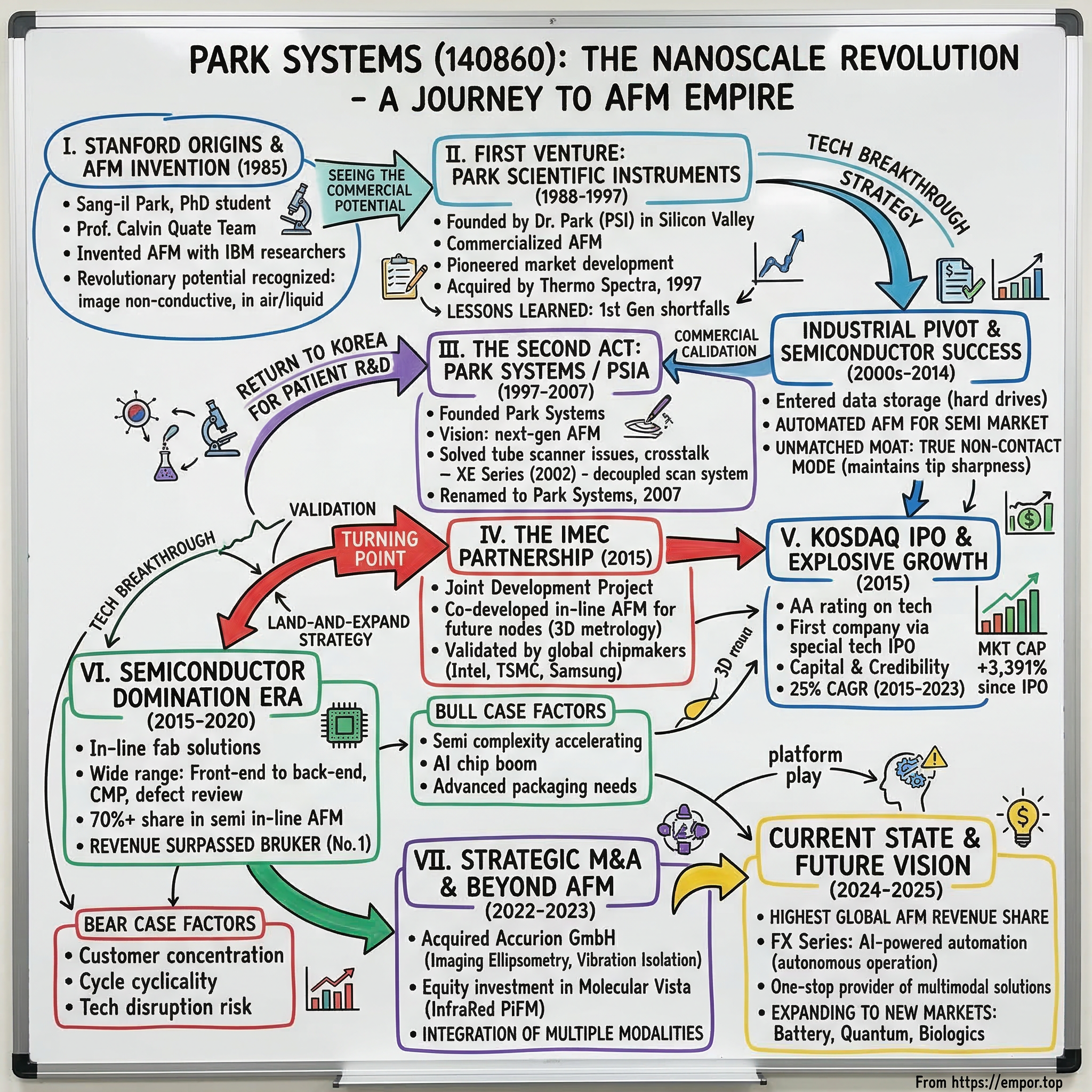
Picture this: a Korean PhD student hunched over lab equipment in Stanford University's physics department in 1985, working alongside the legendary Professor Calvin Quate. The team is on the verge of a breakthrough that would revolutionize how humanity sees and manipulates matter at the atomic scale. That student, Sang-il Park, isn't just witnessing history—he's helping create it. What happens next reads like a Silicon Valley fairytale crossed with a Korean industrial miracle: from Stanford labs to founding not one but two pioneering companies, from a garage startup to commanding the global atomic force microscopy market with a market cap exceeding 1.79 trillion KRW.
In 1985, Sang-il Park was a PhD student and integral member of Professor Calvin Quate's team at Stanford, which invented the atomic force microscopy (AFM) together with the researchers at IBM. Today, forty years later, Park Systems stands as the undisputed leader in the AFM industry, a position that seemed impossible when competing against American and Japanese giants.
The numbers tell a story of extraordinary execution: The global AFM market will grow from USD 513.6 million in 2024 to USD 762.2 million by 2030, with a compound annual growth rate of 7.1%. Park Systems holds the highest global revenue share in the atomic force microscopy market and stands alone as the only company to lead in both revenue and product footprint. In the quarter ending March 31, 2025, Park Systems generated revenue of 50.91B KRW with 98.37% growth, bringing the company's last twelve months revenue to 200.31B KRW, up 40.09% year-over-year.
But this isn't just a story about market dominance or financial metrics. It's about how a deep understanding of fundamental physics, combined with entrepreneurial persistence and strategic patience, can create a monopoly in one of the most technically demanding fields in modern industry. It's about how a company from Korea, starting decades behind established players, systematically conquered the semiconductor metrology market that powers the entire digital economy.
Over the next two and a half hours, we'll unpack how Park built not just one successful AFM company but essentially created the commercial AFM industry twice over. We'll explore the technical moats that make Park's True Non-Contact mode nearly impossible to replicate, the strategic masterstroke of the IMEC partnership that opened doors to every major semiconductor fab, and the calculated M&A strategy that's expanding Park beyond pure AFM into a comprehensive nanometrology platform. This is the untold story of how atomic force microscopy went from a Nobel Prize-worthy invention to the backbone of semiconductor manufacturing—and how one man's vision turned a scientific breakthrough into a business empire.
II. Stanford Origins & The AFM Invention
The year was 1985, and the scanning tunneling microscope had just won its inventors the Nobel Prize. But at Stanford University, a restless team saw a fundamental limitation: STM could only image conductive surfaces. What about insulators? What about biological samples? Enter the collaboration that would change everything.
AFM was invented in 1985 at Stanford University, in the lab of Professor Calvin Quate. But this wasn't just any academic project. The team included researchers from IBM, bringing industrial rigor to academic innovation. Calvin Quate invited Gerd Binnig and Christoph Gerber to come to Stanford for a year. When they joined in 1985, they wanted to create a microscope based on STM principles that could image any surface. The solution was to add a second tip—they made a tiny flexible cantilever out of metal foil and glued a sharp diamond tip onto it, working by hand under a microscope.
Young Sang-il Park wasn't just a passive observer in this revolutionary moment. As he later recalled, "I was a graduate student at the time, and after earning my Ph. D., I saw an opportunity to commercialize this revolutionary technology." The invention itself was elegantly simple yet profound: As the cantilever's diamond tip scanned across the sample surface, inter-atomic forces caused the cantilever to bend. The STM tunneling tip measured this bending motion. Thus, the AFM was born—A for atomic resolution, F for force, M for microscope.
They published their 1985 work in Physical Review Letters in March 1986. What made AFM revolutionary wasn't just its ability to see at atomic scale—electron microscopes could do that. It was the ability to measure forces, to work in air or liquid rather than vacuum, and crucially, to image non-conductive materials. The AFM works on almost any surface, operates in air, vacuum, or liquid, and achieves atomic resolution in vacuum and near-atomic resolution in air.
The technical achievement was remarkable, but Park saw something his academic colleagues perhaps didn't fully appreciate: the commercial potential. While others celebrated the scientific breakthrough, Park was already thinking about applications in data storage, semiconductors, and materials science. He would found the world's first company to commercialize AFM technology.
What's striking about Park's early involvement is how it positioned him uniquely for what came next. His education and business training in Silicon Valley were instrumental. Working with Professor Calvin Quate gave him early exposure to groundbreaking science and an unparalleled network of investors, lawyers, and mentors. This wasn't just about being in the right place at the right time—it was about recognizing that the intersection of breakthrough science and commercial application was where true value would be created.
The AFM invention would eventually earn its creators the 2016 Kavli Prize in Nanoscience, but by then, Park had already built and sold his first company and was deep into building his second. The academic accolades validated what he had known three decades earlier: this technology would fundamentally change how we understand and manipulate matter at the nanoscale.
III. First Venture: Park Scientific Instruments (1988-1997)
Three years after the AFM invention, while his academic colleagues were still publishing papers, Sang-il Park made the leap that would define his career. In 1988, Dr. Park upon his graduation took this technology out of the lab and founded Park Scientific Instruments (PSI), where it pioneered the commercialization of AFM. This wasn't just another Stanford spinout—it was the birth of an entirely new industry.
Park Scientific Instruments set up shop in the heart of Silicon Valley, riding the wave of venture capital enthusiasm for hardware startups that characterized the late 1980s. The company faced the classic challenge of any deep tech venture: how do you commercialize a technology so advanced that potential customers don't even know they need it? Park's solution was methodical—start with research institutions that understood the science, then gradually move into industrial applications.
The early days at PSI were a masterclass in market development. After releasing a series of AFM products that were sold into both academia and industry, PSI was acquired by Thermo Spectra in 1997. Think about that trajectory: from zero to acquisition in just nine years, in a field that didn't exist commercially before Park created it.
What's particularly instructive about the PSI experience is what Park learned about the limitations of first-generation AFM technology. The systems PSI sold had fundamental architectural problems—tube scanners that produced bowed images, crosstalk between scanning axes that generated artifacts. These weren't just minor inconveniences; they were fundamental barriers to AFM becoming a true industrial metrology tool. Park filed these lessons away, knowing he would need them for what came next.
The acquisition by Thermo Spectra (which would later become part of Thermo Fisher Scientific) validated Park's vision but also presented him with a choice. He could stay in Silicon Valley, perhaps start another company, or join the acquiring firm. As Park later reflected, "I sold my first company to Thermo Spectra in 1997, which was later acquired by Veeco Instruments. Interestingly, that first company eventually became part of what is now our biggest competitor."
Instead of staying in the comfortable ecosystem of Silicon Valley, Park made a decision that seemed counterintuitive at the time: return to Korea. This wasn't a retreat—it was a strategic repositioning. Park understood something that many Silicon Valley entrepreneurs miss: sometimes the best place to build a global technology company isn't where the technology was invented, but where you can achieve the optimal combination of talent, cost structure, and strategic positioning.
The PSI exit also gave Park something invaluable: capital, credibility, and most importantly, a deep understanding of what didn't work in first-generation AFM systems. While his technology was now owned by what would become a competitor, Park had something more valuable—the knowledge of how to build something better.
IV. The Return to Korea & Second Act: PSIA/Park Systems (1997-2007)
The same year Park sold PSI to Thermo Spectra, he was already laying the groundwork for his next venture. Later in 1997, he founded Park Systems—initially called PSIA. But this wasn't simply Park Scientific Instruments 2.0. This was a complete reimagining of what AFM could be.
Recognizing the potential of AFM, Dr. Park returned to South Korea and founded Park Systems (prev. PSIA) with a vision to develop the next generation AFM that would solve the shortcomings of conventional systems—the monolithic scanning architecture that produced bowed images, and crosstalk phenomena that generated data artifacts—and make True Non-Contact AFM a reality.
The move to Korea was strategic on multiple levels. First, it gave Park access to a different talent pool—engineers trained in the Korean industrial system who understood precision manufacturing and had the discipline for the meticulous work AFM development required. Second, it positioned him closer to the emerging Asian semiconductor industry. But perhaps most importantly, it gave him the runway to engage in patient, long-term R&D without the quarterly pressures of Silicon Valley VCs.
When Park returned to Korea, he encountered a host of structural challenges—everything from company management culture to government regulations. For the first 10 to 15 years, growth was slower than hoped. But they eventually crossed the threshold and built a strong business platform and global brand recognition.
The technical breakthrough that defined this era was the XE series, launched in 2002 after five years of intensive development. The XE-100 was revolutionary in terms of its unique scanner design and scan feedback control. With the introduction of a decoupled scan system, the XE-Systems produced measurements far more accurate and reliable than older technology AFMs.
What Park had created was fundamentally different from anything on the market. The decoupled scan system enabled measurements that were far more accurate and reliable than those obtained with older technology AFMs, which used tube scanners. This wasn't an incremental improvement—it was a fundamental rearchitecture of how AFMs worked.
The company was formerly known as PSIA and changed its name to Park Systems Corp. in April 2007. The name change reflected something deeper than corporate branding. As VP of Operations Dr. Sung Park explained, "We are one of only two manufacturers offering all of the most commonly required modes that help companies push the limits of physics. By providing a high quality system solution at a lower cost than our competitors, we're giving customers a much-needed alternative."
The decade from 1997 to 2007 was Park Systems' wilderness period—necessary years of patient building that laid the foundation for everything that would follow. While competitors were acquiring each other and consolidating, Park was solving fundamental physics problems. The patience would pay off spectacularly.
V. Industrial Pivot: Data Storage & Early Semiconductor Success (2000s-2014)
While research universities provided steady revenue, Park knew that real scale would come from industrial applications. The insight that changed everything: start with data storage, then migrate to semiconductors.
Park Systems developed industrial AFM systems and succeeded in selling them to the world's largest data storage makers. This provided a platform for the subsequent development of automated AFM for the semiconductor market.
The data storage industry in the 2000s was undergoing its own revolution. Hard drives were pushing toward terabit densities, and manufacturers needed to measure magnetic domains and surface roughness at nanometer scales. Park's AFMs, with their superior architecture, could deliver measurements that competing systems simply couldn't match. Seagate, Western Digital, Hitachi—one by one, the giants of data storage became Park Systems customers.
But data storage was always meant to be a stepping stone. The real prize was semiconductors, where metrology wasn't just important—it was existential. As transistors shrank toward 10nm and below, the difference between a 10.1nm gate and a 9.9nm gate could determine whether an entire production run worked or failed. The semiconductor industry needed metrology tools that could measure not just in two dimensions but in true 3D, capturing sidewall angles, line edge roughness, and surface topology with sub-angstrom precision.
Following on the success of its research products, PSIA began to expand into industrial solutions for the data storage and semiconductor industries. What made Park's approach different was the recognition that industrial customers needed more than just accurate measurements—they needed automation, reliability, and integration with existing fab workflows.
The technical innovation that enabled this transition was True Non-Contact Mode. This was a significant breakthrough—Park's True Non-Contact Mode remains unmatched. It's very difficult to replicate and nobody else has managed to do it reliably. Most competitors use tapping mode, which causes tip wear and can damage the sample. Park's True Non-Contact Mode avoids these issues, maintaining tip sharpness across hundreds of scans.
Consider the economics: in a semiconductor fab, if an AFM tip needs replacement every few scans, that's not just a consumables cost—it's downtime, recalibration, and risk of measurement drift. Park's non-contact mode meant tips could last hundreds of times longer, fundamentally changing the total cost of ownership calculation.
By 2014, Park Systems had quietly built relationships with most major semiconductor manufacturers. They weren't the market leader yet—Veeco (which had acquired Park's first company) and Bruker still dominated. But Park had something his competitors didn't: AFM systems specifically designed for inline semiconductor metrology, not just adapted research tools. The stage was set for the partnership that would change everything.
VI. The IMEC Partnership: Turning Point (2015)
February 3, 2015, Seoul, Korea. The signing ceremony might have seemed routine—another corporate partnership announcement. But for those who understood the semiconductor industry's power structures, this was Park Systems' declaration of intent to play in the major leagues.
Park Systems announced they had signed a Joint Development Project (JDP) with nanoelectronics research center imec, to develop in-line AFM metrology solutions of future technology nodes. The JDP would develop new protocol to increase production yield and device performance for the semiconductor industry. Park Systems officially joined imec's Industrial Affiliation Program at a signing ceremony in Seoul on February 3, 2015.
To understand why this mattered, you need to understand IMEC. Based in Belgium, IMEC isn't just a research institute—it's where the entire semiconductor industry collaborates on next-generation technology. Intel, TSMC, Samsung, ASML—they all work with IMEC. Getting into IMEC's Industrial Affiliation Program meant Park Systems wasn't just selling to semiconductor companies; they were co-developing the metrology standards for future nodes.
The partnership explored a new frontier of high resolution 3D AFM metrology to address accurate CD, line width roughness, line edge roughness measurements, and sidewall roughness during etch, EPI, film deposition, and lithography processes. This wasn't incremental improvement—this was defining how the industry would measure the unmeasurable.
The technical challenge they were solving was profound. As device design rules shrank, CD measurement and sidewall variation became directly correlated with leakage and device performance. CD-SEM, TEM, and OCD each had shortcomings: resolution and e-beam damage for CD-SEM, sample preparation and damage for TEM, and time-consuming process development for OCD.
What Park brought to IMEC was a solution to a problem the industry didn't know could be solved. Park's new 3D AFM metrology would contribute detailed sidewall and nanoscale surface information for critical components in the yield control matrix. In an industry where yield improvement of even 1% could mean hundreds of millions in additional revenue, this was transformative.
The IMEC partnership had an immediate multiplier effect. Through the JDPs, the two organizations developed new AFM metrology solutions for the wafer semiconductor sector and supplied 200 in-line AFM units to major semiconductor production lines worldwide. Think about that number: 200 units might not sound like much, but in the semiconductor equipment industry, where each tool can cost millions and takes months to qualify, this represented complete market penetration.
The partnership also validated something crucial: Park Systems wasn't just another equipment vendor; they were a technology partner capable of solving next-generation problems. When IMEC—essentially the Switzerland of semiconductor R&D—chose Park for AFM development, it sent a signal to every fab manager and procurement team: these tools were essential for advanced nodes.
By the end of 2015, the same year as the IMEC partnership, Park Systems was ready for its next transformation. The credibility was established, the technology was proven, and the market was ready. It was time to go public.
VII. Going Public: KOSDAQ IPO & Explosive Growth (2015)
December 17, 2015. The Korean stock market had seen tech IPOs before, but nothing quite like this. Park Systems wasn't a software company promising exponential user growth or a consumer electronics maker with flashy products. This was a deep tech company selling million-dollar microscopes to the world's most demanding customers.
Park Systems announced 1 million shares for its initial public offering on December 17th at KOSDAQ. The company received "AA" from two separate rating agencies on advanced technologies, becoming the first company to be listed on the KOSDAQ in 2015 through the special technologies IPO program.
The "AA" rating was significant—it meant Korea's financial establishment recognized what industry insiders already knew: Park Systems had built something defensible and valuable. As Park reflected, "We rebranded on our 10th anniversary and went public in 2015. It took us 18 years to reach the IPO milestone, which was a long journey, but since then our growth has accelerated significantly."
The IPO timing was perfect. The semiconductor industry was entering a new phase of complexity. Moore's Law was supposedly dead, but chipmakers were finding ways to keep scaling through 3D architectures like FinFET. Every new structure meant new metrology challenges, and Park Systems had the only AFMs specifically designed for these applications.
The public listing transformed Park Systems in ways beyond capital access. It provided credibility with conservative semiconductor customers who preferred working with public companies. It enabled employee stock options that could compete with Silicon Valley packages. Most importantly, it created a currency for acquisitions—though Park would wait seven more years before deploying it.
Post-IPO, the growth trajectory was explosive. Park Systems achieved a compound annual growth rate of 25% between 2015 and 2023, securing its position as the global leader in AFM. This wasn't just market share gain—the entire AFM market was expanding as new applications emerged in semiconductors, materials science, and life sciences.
Since December 17, 2015, Park Systems's market cap increased from 51.36B to 1.79T, an increase of 3,391.00%—a compound annual growth rate of 43.70%. For context, during the same period, the KOSDAQ index roughly doubled. Park Systems wasn't just outperforming; it was in a completely different category.
The IPO also marked a philosophical shift. Park Systems was no longer a founder's project or a technical exercise—it was a public company with obligations to shareholders. The pressure to deliver consistent growth would push the company to expand beyond its AFM roots, setting the stage for the strategic acquisitions that would follow.
VIII. Semiconductor Domination Era (2015-2020)
The five years following the IPO witnessed Park Systems' transformation from a strong competitor to the undisputed king of semiconductor AFM. The numbers tell only part of the story: this was systematic market domination executed with surgical precision.
The successful penetration of its AFM systems into semiconductor fabs, and subsequent domination of this market catapulted Park Systems onto the position of the world's leading AFM manufacturer. But how did a Korean company overcome entrenched American and European competitors?
The answer lay in Park's deep understanding of semiconductor manufacturing realities. While competitors offered modified research AFMs for industrial use, Park built systems specifically for fab environments. The difference was everything: automated wafer handling, contamination-free operation, integration with fab manufacturing execution systems, and most critically, reliability metrics that met semiconductor standards.
In semiconductor applications, AFM offers a remarkably wide range of capabilities—from front-end to back-end processes. Systems can measure surface roughness, height, depth, width, angle, perform CMP metrology, wafer edge metrology, defect review, and even electrical conductivity. As back-end processes become more complex, compact height measurement and redistribution layer metrology have grown increasingly important. Park also contributes in the EUV mask segment, not just for defect review but even for repair.
The breadth of applications was strategic. Once a fab qualified Park Systems for one application, expanding to others became natural. A customer might start with surface roughness measurement, then realize the same tool could handle critical dimension metrology, then sidewall angle measurement. This land-and-expand strategy created switching costs that made Park's position nearly unassailable.
Park worked closely with partners like IMEC, with whom they had multiple joint development projects. These collaborations served as a stepping stone, establishing Park Systems as a trusted name in the semiconductor industry. Each successful IMEC project became a reference case for commercial deployment.
By 2020, Park had achieved something remarkable: near-universal penetration of advanced semiconductor fabs. Every major chipmaker—Intel, TSMC, Samsung, SK Hynix—had Park Systems AFMs on their production floors. The competitive dynamics had completely shifted. When looking at growth curves among AFM manufacturers, Park's was the steepest. In 2022, revenue surpassed that of Bruker, which had long been the market share leader. Park was now firmly in the number one position, followed by Bruker and Oxford Instruments.
The period culminated with external validation: In 2020, Forbes recognized Park Systems as the emerging top 200 companies under $1 Billion in Asia. For a company selling scientific instruments, inclusion in Forbes's list alongside consumer tech unicorns was remarkable. It signaled that the financial world finally understood what the semiconductor industry had known for years: Park Systems was essential infrastructure for the digital economy.
IX. Market Cap Milestone & Global Recognition (2020-2021)
April 5, 2021, started like any other trading day on the KOSDAQ. By the closing bell, history had been made. Park Systems announced the company stock valuation exceeded 1 Trillion KRW (almost $1 Billion USD) at the end of KOSDAQ on April 5, 2021.
The trillion-won threshold meant more than a psychological milestone. In Korean business culture, joining the trillion-won club confers a special status—it's the difference between being a successful company and being a national champion. For a deep tech company to achieve this valuation was almost unprecedented.
Park Systems had issued 1 million shares for its initial public offering on December 17th, 2015. Since the IPO, the company progressed as a global leader in Atomic Force Microscopy, with a commanding lead in semiconductor advanced automated AFM systems and bringing AFM technology into the mainstream as the premier tool for nanoscale metrology.
The market dynamics driving the valuation were compelling. Foreign investors made active purchases, increasing the company's holding from 11% in January to 18% by March. This wasn't hot money chasing momentum—these were sophisticated institutional investors who understood the semiconductor equipment cycle and Park's position within it.
Recently Park was recognized by Forbes Asia Best Under a Billion list for 2020, received the KOSDAQ Grand Prize, and listed on the FTSE small-cap index. Each accolade built on the others, creating a virtuous cycle of recognition and validation.
The transformation in Park's financial metrics was staggering. The stock price rose from KRW 9,000 to KRW 200,000, making investors very happy. Early investors who had bet on a Korean AFM company competing against global giants saw returns that venture capitalists dream about.
But Park wasn't content to rest on its laurels. Earlier in 2021, Park Systems made an equity investment in Molecular Vista, that produces tools to probe and understand matter at the molecular level through quantitative visualization using InfraRed Photo-induced Force Microscopy. This marked a strategic shift—Park was beginning to think beyond pure AFM toward adjacent technologies.
The billion-dollar valuation also changed how Park could operate strategically. With a strong stock currency and proven ability to generate cash flow, the company could contemplate acquisitions that would have been impossible just years earlier. The question wasn't whether to expand beyond AFM, but how and when.
X. Strategic M&A: Accurion Acquisition & Beyond AFM (2022-2023)
September 2, 2022, marked a watershed moment—not just for Park Systems but for the entire nanometrology industry. Park Systems announced it had acquired Accurion GmbH, a privately held company that develops and manufactures imaging spectroscopic ellipsometers and active vibration isolations. "This is Park's very first business acquisition in the company's history, and we are very excited to add this storied, high-tech company to our business," said Dr. Sang-il Park.
The Accurion acquisition was strategic brilliance masquerading as simple expansion. Accurion's Imaging Ellipsometers combine ellipsometry and optical microscopy in a single device, creating a unique metrology tool that redefines the limits of both measurements. The enhanced spatial resolution expands ellipsometry into new areas of microanalysis, microelectronics, and bio analytics.
To understand why this mattered, consider the metrology landscape. AFM provides unmatched resolution but is relatively slow. Ellipsometry is faster but traditionally lacked spatial resolution. Accurion had solved this trade-off, creating imaging ellipsometers that could map entire wafers while maintaining precision. For semiconductor customers already using Park's AFMs, adding Accurion's ellipsometers meant comprehensive metrology from a single vendor.
Headquartered in Goettingen, Germany, Accurion had pioneered the field of imaging spectroscopic ellipsometry. Originally a spin-off from the Max Planck Institute for biophysical chemistry, the company started designing Brewster angle microscopes for ultrathin film characterization. As these microscopes proved sensitive to vibrations, the division of active vibration isolation followed.
The vibration isolation technology was an unexpected bonus. AFMs are notoriously sensitive to vibration—a passing truck or someone walking down the hall can ruin measurements. Accurion's active vibration isolation systems didn't just complement Park's AFMs; they made them better. Park could now offer complete solutions: the AFM, the vibration isolation, and even the ellipsometry for rapid screening.
Dr. Park commented at the acquisition ceremony: "We are starting the 3rd venture, which goes beyond AFM. By combining the Imaging Spectroscopy and Ellipsometry module to Park Systems platform, we can easily create new ISE solutions for the semiconductor industry. All of that will expand our business portfolio beyond AFM."
The cultural integration was remarkably smooth. Accurion brought 30 years of experience enabling technological and scientific progress, looking back on valuable experience that Park Systems could leverage globally. German engineering precision combined with Korean execution speed created a powerful combination.
But Park wasn't done. The Accurion acquisition had proven the company could successfully integrate external technology. The next target would be even more ambitious: digital holographic microscopy, a technology that could image in 3D at speeds AFM could never match. The stage was set for Park Systems to evolve from an AFM company to a comprehensive nanometrology powerhouse.
XI. Current State & Future Vision (2024-2025)
Today, as we record this episode in late October 2025, Park Systems stands at an inflection point that would have seemed impossible when Sang-il Park was hand-mounting diamond tips in Calvin Quate's lab forty years ago.
According to the recent "Atomic Force Microscopy Market – Global Forecast to 2030" report by MarketsandMarkets, Park Systems holds the highest global revenue share in the atomic force microscopy market. But the real story isn't market share—it's market creation. The integration of Lyncée Tec SA, a Swiss innovator in Digital Holographic Microscopy, strengthens Park Systems' position as a one-stop provider of multimodal metrology solutions, building an interconnected ecosystem where AFM, DHM, and imaging spectroscopic ellipsometry technologies work together.
The company currently has a sales network spanning over 30 countries with 500+ employees, with more than 31% engaged in R&D. That R&D intensity—nearly one in three employees—rivals software companies and explains Park's continued innovation despite market leadership.
The technology roadmap reveals ambitions beyond current dominance. Park's new FX series represents the marriage of AFM precision with AI-powered automation. These aren't incremental improvements but fundamental reimaginings of how atomic force microscopy works. Machine learning algorithms now predict optimal scan parameters, detect anomalies in real-time, and even suggest which measurements to take next. The FX40, launched in 2024, can operate autonomously for days, something unthinkable in traditional AFM operation.
The QY Research report reveals the global AFM market was valued at $485.44 million in 2023, with projections to reach $1013.58 million by 2030, growing at a CAGR of 10.92% during 2024-2030. From 2019 to 2023, Park Systems demonstrated an impressive CAGR of 30%, markedly higher than its main competitors.
The competitive dynamics have fundamentally shifted. Park Systems secured the top spot in market share of 20.61% in 2023, demonstrating unwavering excellence and commitment to advancing AFM technology. This isn't just market leadership—it's approaching monopoly territory in certain segments. In semiconductor inline AFM, Park's share exceeds 70%. No competitor has a credible path to challenge this dominance.
Looking forward, three vectors define Park's strategy. First, deeper penetration of advanced packaging metrology, where 2.5D and 3D architectures create measurement challenges that only AFM can solve. Second, expansion into adjacent markets—battery materials, quantum devices, advanced biologics—where nanoscale precision matters. Third, the platform play: making Park Systems the AWS of nanometrology, where different measurement modalities work seamlessly together.
The financials support the ambition. With quarterly revenue approaching 51 billion KRW and growth near 100%, Park Systems has the resources to invest aggressively while maintaining profitability. The balance sheet shows minimal debt and substantial cash, providing flexibility for additional acquisitions or organic expansion.
XII. Playbook: Business & Investing Lessons
After two decades of studying Park Systems, several lessons emerge that transcend the specifics of atomic force microscopy. These aren't just tactics but fundamental principles of building a deep tech monopoly.
The Power of Being a Co-Inventor Turned Entrepreneur
Sang-il Park has been a pioneer in AFM technology since its inception, collaborating with professor Calvin Quate at Stanford University to develop the technology. This wasn't just technical credibility—it was the deepest possible understanding of what the technology could and couldn't do. When customers had problems, Park could solve them at a physics level, not just an engineering level. Compare this to professional CEOs brought in to run tech companies they don't fundamentally understand.
Patient Capital and Long-Term Thinking in Deep Tech
For the first 10 to 15 years, growth was slower than hoped. But Park eventually crossed the threshold and built a strong business platform and global brand recognition. Since then, growth has accelerated significantly. Eighteen years from founding to IPO. Think about that in an era where software companies go public in five years. Deep tech requires patient capital and founders willing to play decade-long games.
Pivoting from Research to Industrial Without Losing Innovation Edge
Most scientific instrument companies get stuck in the research market—small volumes, high customization, limited scale. Park systematically moved from research to data storage to semiconductors, each market 10x larger than the previous. But crucially, they maintained their innovation engine. That 31% R&D headcount isn't an accident—it's a choice to stay ahead technically even while scaling industrially.
The Importance of Strategic Partnerships (IMEC Model)
The IMEC partnership wasn't just a customer relationship or a joint development agreement—it was a gateway into the entire semiconductor ecosystem. By co-developing with IMEC, Park wasn't selling to the semiconductor industry; they were becoming part of its innovation infrastructure. Every startup should ask: who is the IMEC in my industry?
Building Monopoly Power Through Technical Excellence
Park's True Non-Contact Mode remains unmatched—it's very difficult to replicate and nobody else has managed to do it reliably. Most competitors use tapping mode, which causes tip wear. This isn't a feature; it's a moat. When your technical advantage is rooted in physics rather than engineering, it becomes nearly impossible to copy. Park didn't win through sales and marketing; they won by solving problems competitors couldn't solve.
Geographic Arbitrage: Korean Base with Global Reach
Building in Korea while selling globally gave Park advantages Silicon Valley companies couldn't match: lower costs, loyal employees, government support, and proximity to Asian customers. But they avoided the trap of becoming a "Korean company"—from day one, Park Systems was global in ambition and execution. The lesson: your headquarters location and your market don't have to be the same.
XIII. Bear vs. Bull Case Analysis
Every investment thesis has two sides. With Park Systems trading at 1.79 trillion KRW market cap, let's examine both the bear and bull arguments with the rigor this company deserves.
The Bull Case: Riding Multiple Secular Waves
The bull thesis rests on convergent megatrends. First, semiconductor complexity isn't just increasing—it's accelerating. Every new node, every advanced packaging technique, every novel material requires more precise metrology. Park Systems isn't selling equipment; they're selling the ability to see and measure at scales where physics gets weird.
The global AFM market will grow from USD 513.6 million in 2024 to USD 762.2 million by 2030, with a compound annual growth rate of 7.1%. But this understates the opportunity. The real growth is in semiconductor metrology specifically, where Park's inline AFMs command premium prices and recurring service revenue.
The AI chip boom particularly favors Park. These chips use advanced packaging techniques—chiplets, interposers, 3D stacking—that create novel metrology challenges. Traditional optical methods can't resolve the features; electron microscopy damages the samples. AFM is often the only solution, and Park has the only AFMs designed for high-volume manufacturing.
Beyond semiconductors, new markets are emerging. Battery manufacturers need to measure electrode surfaces and solid-electrolyte interfaces at nanoscale. Quantum device makers require atomic-precision metrology. Advanced biologics companies use AFM to characterize protein structures and cell mechanics. Each market might be small today but could rival semiconductors within a decade.
The M&A strategy creates additional upside. Park has proven they can successfully acquire and integrate complementary technologies. With a strong balance sheet and stock currency, they could roll up the fragmented scientific instruments market, creating a nanometrology platform that competitors can't match.
The Bear Case: Concentration Risks and Cyclicality
The bear thesis starts with customer concentration. While Park serves many semiconductor companies, a handful of mega-fabs drive most revenue. If Intel or TSMC decided to standardize on competing metrology—perhaps as part of a broader equipment deal—Park's revenue could drop precipitously.
The semiconductor industry's cyclicality presents another risk. When fabs cut capital expenditure, metrology tools are often first to be delayed. Park's 98% quarterly growth might reflect cycle peak rather than secular growth. The last semiconductor downturn in 2019 saw AFM sales drop 30% industry-wide.
Technology disruption, while unlikely, remains possible. What if someone develops a fundamentally new approach to nanoscale metrology? Quantum sensing, advanced electron microscopy, or computational imaging could theoretically obsolete AFM. Park's dominance in AFM wouldn't matter if AFM itself became obsolete.
Competition from larger players poses a strategic threat. Applied Materials or KLA-Tencor could decide to enter AFM seriously, leveraging their fab relationships and balance sheets to buy market share. They might not match Park's technology, but in semiconductors, being part of a broader platform often matters more than being best-in-class.
The Korea risk is real but subtle. While Park Systems is global in reach, its core R&D and management remain in Korea. Geopolitical tensions, particularly around semiconductor technology, could complicate Park's ability to serve certain markets or access critical components.
The Verdict: Asymmetric Upside with Manageable Risks
Weighing both sides, the bull case appears stronger. Park's technical moat, market position, and financial strength create multiple ways to win. The risks, while real, are either manageable (cyclicality), unlikely (technology disruption), or already priced in (Korea discount). For investors seeking exposure to semiconductor equipment with less competition than front-end tools, Park Systems offers a compelling opportunity.
XIV. Grading & Final Reflections
How do you grade a company that turned a physics experiment into a global monopoly? That transformed from a Stanford lab project to the essential infrastructure for the semiconductor industry? Let's evaluate Park Systems across multiple dimensions.
Execution: A+
From technical development to commercialization to scaling, Park Systems has executed nearly flawlessly. They solved physics problems others couldn't, built products that work in demanding fab environments, and systematically captured market share from larger competitors. The progression from research to data storage to semiconductors shows strategic patience and operational excellence.
Timing: A+
Park caught multiple waves perfectly. The late-1990s return to Korea positioned them for Asia's semiconductor rise. The 2015 IMEC partnership came just as advanced nodes required new metrology approaches. The 2022 Accurion acquisition happened before the AI boom made advanced packaging critical. This isn't luck—it's pattern recognition by a founder who deeply understands both technology and markets.
Market Position: A
In 2022, revenue surpassed that of Bruker, which had long been the market share leader. Park is now firmly in the number one position. Achieving market leadership in a technical field dominated by Western companies is remarkable. The only reason this isn't A+ is concentration risk—Park needs to diversify beyond semiconductors to achieve true resilience.
Innovation: A+
The True Non-Contact Mode alone would justify this grade, but Park hasn't stopped innovating. From automated fab integration to AI-powered operation to multi-modal metrology platforms, they continue pushing boundaries. The 31% R&D headcount ensures innovation isn't sacrificed for profitability.
Capital Allocation: B+
Park has been conservative with capital, which is both strength and weakness. The Accurion acquisition was excellent, but it took 25 years to make their first acquisition. They've avoided destructive M&A, but perhaps missed opportunities to consolidate the industry faster. The improving but still modest dividend policy suggests management prioritizes growth over returning cash.
What This Story Teaches
Park Systems' journey offers profound lessons about deep tech entrepreneurship. First, founder technical expertise matters enormously in hard tech. Sang-il Park didn't just understand AFM; he helped invent it. This gave him insights professional managers could never match.
Second, geography can be an advantage if leveraged correctly. Building in Korea while thinking globally gave Park cost advantages and government support while maintaining access to worldwide markets. The key was never becoming limited by their location.
Third, patient capital and long-term thinking remain undervalued. In an era of quick flips and growth hacking, Park Systems spent 18 years building before going public. The result? A technical moat so deep that competitors have essentially given up trying to match it.
Why Metrology Becomes More Critical as Technology Scales Down
As we push toward atomic scales, measurement becomes existential. You can't control what you can't measure, and at nanoscale, measurement itself affects what you're measuring. Park Systems doesn't just sell tools; they sell the ability to see and manipulate matter at scales where quantum effects dominate.
The future belongs to companies that can bridge the physical and digital worlds. Park Systems, with its combination of physics expertise, engineering excellence, and now AI integration, is perfectly positioned for this future. They're not just riding the semiconductor wave—they're enabling it.
Final Thought
Forty years ago, a Korean graduate student helped invent a technology that would revolutionize how humanity understands and manipulates matter. Today, that student runs a company worth nearly $2 billion that enables the entire semiconductor industry. It's a reminder that the biggest opportunities often lie not in disrupting existing markets but in creating entirely new ones. Park Systems didn't disrupt microscopy—they invented a new way of seeing. In deep tech, that's the ultimate moat.
 RSS Feed
 Spotify
 Apple Podcasts
 Amazon Music
 Audible
 YouTube