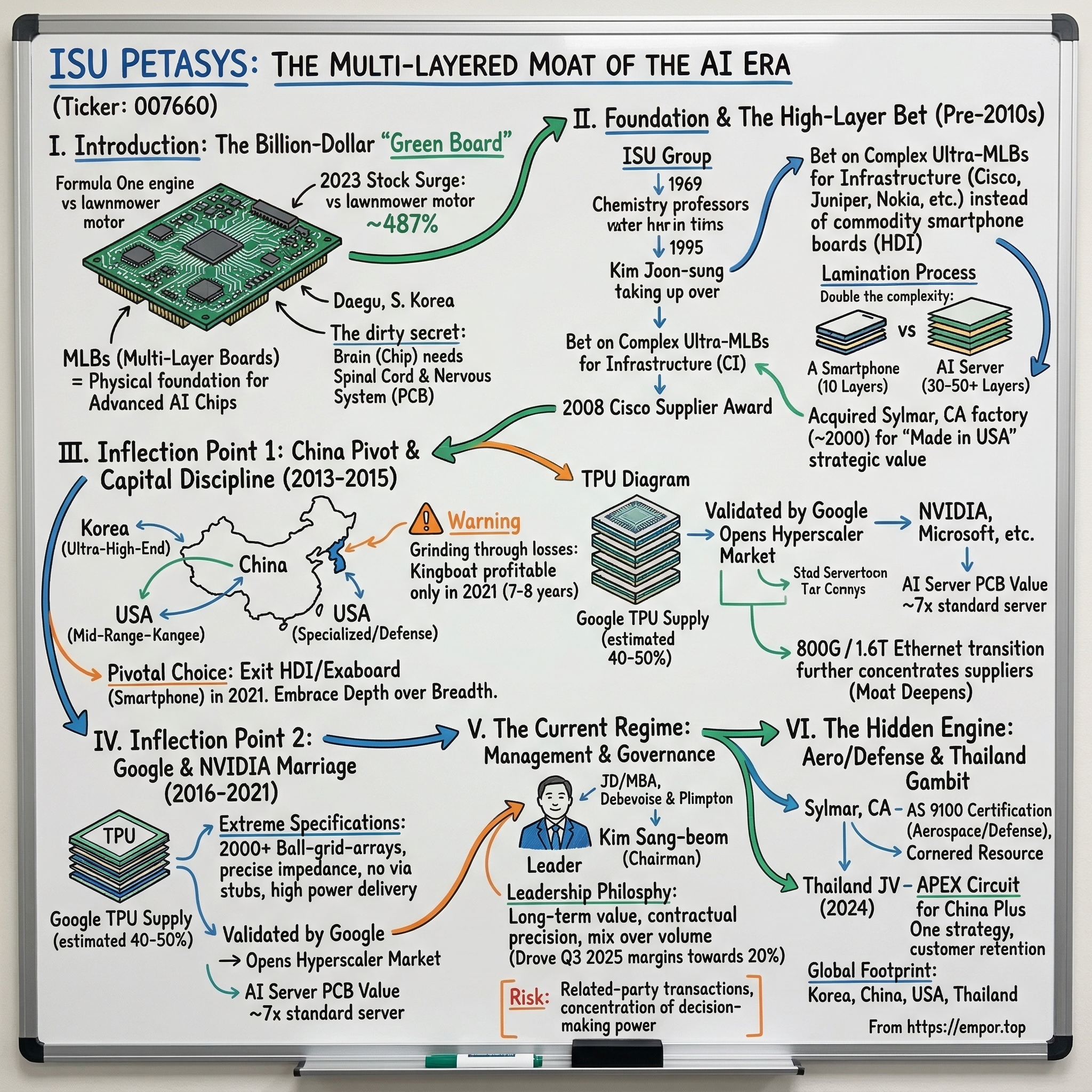
ISU Petasys: The Multi-Layered Moat of the AI Era
I. Introduction: The Billion-Dollar "Green Board"
Picture the scene: it is the summer of 2023, and every investor on earth is scrambling to buy NVIDIA. Jensen Huang's leather jacket is on the cover of magazines. Microsoft is pouring billions into OpenAI. Semiconductor stocks are ripping. The AI gold rush is well and truly underway. But halfway around the world, in the industrial city of Daegu—South Korea's third-largest metro, a city better known for its textile mills and apple orchards than for cutting-edge technology—a fifty-year-old company that most people have never heard of is quietly experiencing the stock run of a lifetime.
ISU Petasys, ticker 007660 on the Korea Exchange, saw its shares surge nearly 487 percent in 2023. Bloomberg ran a stunned headline about a "little-known hardware firm" riding the AI boom. Korean retail investors, the famously aggressive "ants" of the KOSPI, piled in. And yet, outside a small circle of institutional analysts and a handful of sharp-eyed global fund managers, almost nobody could clearly explain what this company actually did—or why its stock was behaving like a high-growth software company rather than an industrial manufacturer.
Here is the answer, stated as simply as possible: ISU Petasys makes the physical boards that the most advanced AI chips in the world sit on. Not the silicon. Not the software. The actual, tangible, green-colored printed circuit boards—multilayer laminations of copper and resin—that form the nervous system connecting every transistor to every power rail, every memory bus to every high-speed interconnect, inside the servers that train the frontier AI models reshaping civilization.
Now, that description might sound boring. "Circuit boards" conjures images of the flat green rectangles visible inside a desktop computer—commodity components stamped out by the millions in factories across Guangdong. But the boards ISU Petasys makes are to those commodity PCBs what a Formula One engine is to a lawnmower motor. They share the same basic concept. The execution, the precision, the sheer difficulty of manufacturing—these are in entirely different universes.
Why does this matter? Because there is a dirty little secret in the semiconductor industry that rarely makes the front page. You can design the most brilliant chip architecture ever conceived. You can spend two billion dollars on a cutting-edge fabrication process at TSMC. You can package it with the most advanced HBM memory Samsung or SK Hynix can produce. And none of it works unless the printed circuit board it mounts to can handle the signal integrity, power delivery, and thermal management that the chip demands.
Think of it this way: the chip is the brain. The PCB is the spinal cord and nervous system. A brilliant brain connected to a damaged nervous system cannot function. And as AI accelerators have grown exponentially more complex—more I/O pins, higher data rates, greater power draw—the boards they require have become exponentially harder to manufacture.
A smartphone might need a ten-layer PCB. Think of that as a ten-story apartment building—relatively straightforward to construct. A standard server motherboard might need fourteen to eighteen layers. That is a mid-rise office tower. But the boards inside an NVIDIA DGX system or a Google TPU pod now require thirty, forty, sometimes more than fifty layers of precision-laminated copper and dielectric material, each layer aligned to within twenty-five microns of the others—about a third the width of a human hair—pressed together under enormous heat and pressure without a single defect. That is a hundred-story supertall skyscraper, built to earthquake-proof tolerances, where a millimeter of error anywhere in the foundation dooms the entire structure.
The number of companies on earth that can reliably manufacture these boards at scale can be counted on one hand. ISU Petasys is among the top two or three, alongside American firm TTM Technologies and a handful of Taiwanese and Japanese specialists.
The thesis of this deep dive is what might be called the "Complexity Moat." In most hardware businesses, technology improvements make products cheaper and easier to manufacture over time—Moore's Law drives costs down. In the high-layer PCB business, the opposite is true. Every generation of faster, more powerful AI silicon demands a more complex board beneath it. The moat does not erode with time. It deepens. And ISU Petasys has spent decades—long before anyone was talking about artificial intelligence—building the chemical processes, the manufacturing expertise, and the global factory footprint to exploit exactly this moment.
The story begins in the factories of Daegu. It runs through a prescient acquisition in California, a risky bet on China, a pivotal marriage with Google, and a management philosophy that prizes disciplined complexity over commodity volume. It ends—or rather, it continues—in a world where every new frontier AI model trained on the planet depends, at the most fundamental physical level, on the boards that come out of ISU Petasys's lamination presses. This is a company hiding in plain sight at the foundation of the AI revolution. And understanding how it got there—the decisions made, the risks taken, the patience required—is one of the most instructive business stories of the 2020s.
II. Foundation and The High-Layer Bet (Pre-2010s)
To understand ISU Petasys, you first have to understand the ISU Group, and to understand the ISU Group, you have to understand a peculiar corner of Korean capitalism where chemistry professors, central bankers, and circuit board engineers somehow converge.
It started in 1969, when a group of chemistry professors at Ewha Womans University in Seoul founded ISU Chemical—a specialty chemicals company born from academic research. It was a modest spin-off, the kind of enterprise that in many countries would have stayed small. But this was South Korea in the era of rapid industrialization, when the government was actively encouraging the formation of industrial groups that could absorb Western technology and scale it for export. ISU Chemical grew, expanded into new chemical formulations, and gradually assembled a portfolio of related businesses.
In 1995, the company found a transformative new owner: Kim Joon-sung. His resume reads like a compressed history of modern Korea itself. He had served as a governor of the Bank of Korea—the equivalent of chairing the Federal Reserve. He had been South Korea's Finance Minister. He had chaired Samsung Electronics and later led Daewoo before its spectacular collapse in 1999. By the time he acquired the ISU Group, he was one of the most experienced industrial executives in the country, a man who had seen both the heights and the catastrophic lows of Korean conglomerate capitalism. Under his stewardship, ISU expanded into a diversified mid-sized group—what might be called a "chaebol-lite"—with subsidiaries spanning chemicals, biopharma, construction, and electronics.
The PCB business came into the fold in 1995 as well. The company that would become ISU Petasys had been founded in Daegu on February 14, 1972, as a printed circuit board manufacturer. For its first two decades, it was a fairly standard participant in Korea's booming electronics supply chain—making boards for the telecommunications and computing equipment that Korean and global OEMs were producing at accelerating scale. The formal renaming to ISU Petasys came in March 2002, marking its integration into the ISU Group identity and its ambitions beyond mere contract manufacturing.
But the strategic choice that would define the company's future was made long before the AI era—and it was a choice defined by what ISU decided not to do. While Korean electronics giants like Samsung Electro-Mechanics and LG Innotek chased the enormous volumes of the smartphone revolution—investing heavily in HDI, or High Density Interconnect boards, the thin, compact PCBs that go inside every iPhone and Galaxy device—ISU made a different bet entirely. It focused on ultra-multilayer boards, known in the industry as MLBs. These are the thick, heavy, precisely engineered boards used in network routers, data center switches, supercomputers, and other infrastructure equipment. The kind of boards that no consumer ever sees. The kind of boards where each unit costs not pennies, but hundreds or even thousands of dollars.
To understand why this was such a consequential decision, it helps to understand what "layers" actually mean in PCB manufacturing and why more layers are exponentially harder to produce. A PCB is fundamentally a sandwich: alternating layers of copper (which carries electrical signals and power) and dielectric material (an insulating resin, typically fiberglass-reinforced epoxy, which separates the copper layers and provides structural rigidity). A four-layer board has four copper layers and three dielectric layers between them—easy enough. You laminate them together in a single press cycle, drill your holes, plate them with copper, etch your circuit patterns, and you are done.
Now scale that up. A sixteen-layer board requires multiple lamination cycles—you cannot simply stack sixteen layers and press them all at once, because the alignment tolerances and thermal stresses would be uncontrollable. Instead, you build up the board in stages: laminate a core set of layers, drill and plate vias (the tiny holes that connect one layer to another), then laminate additional layers on top, drill again, plate again, and repeat. Each cycle introduces new opportunities for misalignment, contamination, or delamination. The chemistry of the dielectric material must be controlled with extraordinary precision: its dielectric constant (a measure of how it affects electrical signal speed) and dissipation factor (a measure of how much signal energy it absorbs) must remain uniform across the entire board, across every layer, because at the data speeds modern electronics operate at—tens of gigahertz—even tiny variations cause impedance mismatches that corrupt data.
By the time you reach thirty or forty layers, the manufacturing challenge is qualitatively different from anything in the lower layer counts. Registration—the alignment of features from one layer to the next—must be maintained to within twenty-five microns across a board that might be six hundred millimeters long, through multiple press cycles at temperatures exceeding 180 degrees Celsius. The vias that connect layers become tall and narrow—high "aspect ratio" in engineering terms—and plating copper uniformly inside these deep, narrow holes requires specialized chemistry and process control that has taken companies decades to perfect. And the yields drop dramatically. Each additional lamination cycle multiplies defect opportunities. If a single via out of ten thousand is improperly plated, or a single layer out of forty is misregistered, the entire board—which may have consumed hundreds of dollars of materials and hours of processing time—becomes scrap.
ISU Petasys mastered this chemistry early. By the 2000s, while competitors were scaling up smartphone PCB lines for volume production, ISU was refining its processes for the twenty-to-thirty-layer boards that Cisco, Juniper, Nokia, and Ericsson needed for their networking equipment. In 2008, the company won Cisco's Supplier of the Year award—a meaningful validation that it had reached the top tier of global MLB manufacturers, competing head-to-head with American and Japanese incumbents. This was not a participation trophy. Cisco's supply chain is among the most rigorous in the networking industry, with supplier evaluation processes that assess not just product quality but delivery reliability, cost competitiveness, engineering responsiveness, and the ability to support rapid design iterations. Winning Supplier of the Year meant that ISU had outperformed dozens of competitors—many of them larger, better capitalized, and more established—on every dimension that Cisco's procurement team measured.
The award also signaled something broader about ISU's competitive positioning. In the 2000s, the high-end MLB market was dominated by a handful of American and Japanese companies: TTM Technologies and Sanmina in the US, Ibiden and CMK in Japan. Korean PCB manufacturers were generally perceived as mid-tier players—capable but not at the cutting edge. The Cisco recognition marked the moment when ISU broke through that perception barrier and established itself as a genuine peer of the global leaders. It would take another decade for the market to fully appreciate the significance of that shift—but the foundation was being poured.
And then there was the move that, in retrospect, looks like a twenty-year-old masterstroke. Around 2000, ISU acquired a factory in Sylmar, California, establishing ISU Petasys Corp as its American subsidiary. At the time, this looked like a straightforward business decision: having a US manufacturing presence allowed faster turnaround for American customers who needed quick-turn prototypes and low-volume, high-mix production runs. The Sylmar facility was not going to compete on scale with Korean or Chinese factories. But it gave ISU something that would prove invaluable in a later era of geopolitical tension: a "Made in USA" high-end PCB plant, AS 9100 certified for aerospace and defense work, located on American soil, staffed by American workers, and eligible for the US government contracts and defense programs that increasingly require domestic sourcing.
In the world of 2000, this was a customer convenience—a way to offer faster lead times and local engineering support to Cisco, Juniper, and other American networking companies headquartered within driving distance of Sylmar. In the world of 2025, with US-China decoupling reshaping global supply chains, the CHIPS Act pouring tens of billions into domestic semiconductor manufacturing, and the Pentagon increasingly mandating domestic sourcing for defense electronics, it is a cornered resource—an asset whose strategic value has grown far faster than anyone who approved the original acquisition could have imagined. The Sylmar factory is a time machine: a decision made twenty-five years ago for mundane operational reasons has become a strategic weapon in a geopolitical contest that did not exist when the ink dried on the purchase agreement.
The foundation was laid. ISU had chosen complexity over volume, infrastructure over consumer, and multilayer mastery over commodity scale. What the company needed next was for the market to validate that bet—and it would, though not before ISU took one more calculated gamble, this time across the Taiwan Strait.
III. Inflection Point 1: The China Pivot and Capital Discipline (2013-2015)
In November 2013, ISU Petasys made the kind of move that, at the time, barely registered with anyone outside the PCB industry. The company acquired a sixty percent stake in Kingboat Technology Limited, gaining control of a multilayer PCB factory in Hunan province, China. The facility had previously been part of MFS Technology's operations and had connections to Tripod Technology, one of Taiwan's major PCB manufacturers. By the standards of global M&A, it was a modest deal. But it was a move pregnant with strategic implications that would take nearly a decade to fully materialize.
To appreciate the context, consider the state of the global PCB industry in 2013. China was rapidly becoming the center of gravity for PCB manufacturing, already accounting for roughly forty-five percent of global production and climbing. The forces were irresistible: lower labor costs, proximity to the consumer electronics assembly ecosystem centered in Guangdong and the Yangtze River Delta, and massive government subsidies for the electronics industry. For a Korean PCB manufacturer, the question was not whether to have a China presence, but on what terms.
ISU's answer was deliberately conservative. Unlike some competitors who plunged into China seeking to capture the high-volume, low-margin consumer PCB market, ISU positioned the Kingboat factory specifically for mid-range multilayer work: twelve-to-twenty-layer boards for traditional networking and telecommunications equipment. This was solid, workmanlike production—nothing flashy—but it was well above the commodity PCB segment where Chinese domestic producers were already competing on razor-thin margins.
What made the acquisition strategically elegant was the production tiering it enabled across ISU's now three-continent manufacturing network. With factories in Korea, China, and the United States, ISU could allocate work with surgical precision. Korea handled the ultra-high-end: the thirty-plus-layer boards for supercomputing and, eventually, AI applications, where margins were fattest and the manufacturing tolerances were tightest. China handled the mid-range: networking and telecom boards where price competition was fiercer but volumes were reliable. And the United States handled the specialized: quick-turn prototypes, aerospace and defense work, and the high-mix, low-volume runs that American customers needed for development cycles.
Think of it as a restaurant group that owns a Michelin-starred fine dining establishment, a solid mid-market bistro, and a specialty catering operation. Each kitchen serves a different clientele, with different expectations and different economics, but the group benefits from shared procurement, shared quality systems, and the ability to refer customers across the portfolio. A company like Cisco might need ultra-high-layer backplane boards for its flagship routers manufactured in Korea, mid-range boards for its volume switches manufactured in China, and fast-turn prototypes for next-generation designs manufactured in California—and ISU could serve all three needs from its own facilities. This breadth of capability, spanning the full complexity spectrum across multiple geographies, gave ISU a customer stickiness that single-factory competitors could not match.
The Kingboat acquisition was not without pain—and significant pain at that. The Chinese subsidiary recorded operating losses of ten to twenty billion Korean won annually through 2020. That is seven consecutive years of red ink, a grinding, patience-testing stretch that would have prompted most boards of directors to write off the investment and move on.
But ISU held on, gradually transforming the customer base from primarily Taiwanese clients—who had come with the factory—to American companies. By 2021, approximately seventy percent of the Hunan factory's sales came from US customers, a remarkable transformation driven by the same US-China trade tensions that were reshaping every supply chain on the planet. American networking companies that had been sourcing from purely Chinese suppliers began looking for alternatives that were technically Chinese-manufactured but owned and managed by allied-nation companies. ISU's Korean ownership of a Chinese factory hit a sweet spot. The subsidiary finally turned profitable in the second quarter of 2021, nearly eight years after the acquisition.
Seven or eight years to profitability. That number alone tells you something important about ISU's management culture and its ownership structure. No American public company with quarterly earnings pressure and activist investors breathing down its neck could have sustained that timeline. ISU could, because the ISU Group's holding company structure and its controlling family shareholder were willing to absorb short-term losses in service of a long-term strategic vision. Whether you view that as visionary patience or lax governance depends on your perspective—but the outcome, as of 2026, vindicated the patience.
Meanwhile, ISU was making an equally consequential decision about what not to do. The company had operated an HDI and flexible PCB subsidiary called ISU Exaboard, based in Ansan, South Korea, which supplied boards to Samsung Electronics for smartphones. This was the high-volume consumer game that ISU's competitors were playing—and ISU was losing at it. By 2020, after five consecutive years of losses, ISU Exaboard was running revenues of about 121 billion won against an operating loss of nearly eleven billion won. The math was brutal and getting worse: Chinese HDI producers were relentlessly cutting prices, the smartphone market was maturing, and Samsung's procurement team was—understandably—squeezing suppliers on every won of cost.
ISU pulled the plug. ISU Exaboard shut down operations on July 31, 2021. The liquidation was the mirror image of the Kingboat investment. Where the China acquisition was a bet on geographic diversification within ISU's core competency, the HDI exit was a recognition that competing in high-volume consumer PCBs was a losing game for a company whose real advantage lay in complexity, not scale. Samsung Electro-Mechanics had already exited HDI manufacturing in 2019—a strong signal that the economics no longer worked for Korean producers at any scale.
By closing Exaboard and redeploying capital into its MLB operations, ISU was effectively purifying its identity. It would be the company that made the hardest boards in the world, and nothing else. The capital that might have been wasted propping up a dying consumer business would flow instead into expanding the Daegu facilities and investing in the next generation of ultra-high-layer manufacturing processes. It was the kind of discipline that often looks obvious in retrospect but requires genuine conviction in the moment—the willingness to accept a smaller total addressable market in exchange for a much larger share of the most profitable segment within it. In the language of strategy, ISU was trading breadth for depth—and the depth it was choosing happened to be the exact depth that the AI revolution would soon demand.
With a lean, focused cost structure and a global factory network positioned for the coming decade, ISU needed one more ingredient: the right customers to prove that the high-end bet could scale. Those customers were about to come knocking—and they came from a direction that few in the traditional telecom-focused PCB world had anticipated.
IV. Inflection Point 2: The Google and NVIDIA Marriage (2016-2021)
Sometime around 2016, a shift began in the PCB industry that almost nobody outside of a few Korean and Taiwanese factory floors anticipated. For decades, the primary demand driver for high-layer multilayer boards had been telecommunications infrastructure—the routers and switches that Cisco, Juniper, Nokia, and Ericsson sold to telecom carriers and enterprise customers. ISU Petasys had built its business on this demand, and it was a good business. But the growth engine was sputtering.
Telecom equipment refresh cycles were lengthening. The explosive buildout of 4G networks was plateauing, and 5G—while generating excitement—was not yet translating into the kind of massive hardware procurement cycles that moved the needle for board suppliers. Carrier capital expenditure was flattening. For a company that had bet everything on high-end MLB, the plateau in telecom was more than a temporary headwind. It was an existential question: where would the next wave of demand come from?
The answer arrived in the form of a company most people associate with search engines and online advertising, not with hardware procurement: Google.
To understand why this was such a seismic shift, recall that before 2016, the PCB industry had a well-established hierarchy of end markets. Telecom was the premium segment—high layer counts, demanding specifications, good margins. Below that sat enterprise computing—servers and storage with moderate complexity. And at the bottom was consumer electronics—high volume, low margin, intense competition. What nobody anticipated was the emergence of an entirely new tier above telecom: the hyperscaler AI segment, where the complexity requirements would make even the most demanding telecom boards look routine by comparison.
The details of how ISU Petasys became a primary supplier for Google's Tensor Processing Units—the custom AI accelerators that Google designs in-house for machine learning training and inference—have never been fully disclosed publicly. But the contours of the relationship have been pieced together by Korean securities analysts, most notably at Meritz Securities and Hanwha Investment and Securities, who estimated that ISU eventually captured a substantial portion of Google's MLB supply for TPU applications—some estimates ranging as high as forty to fifty percent of Google's total TPU board volume.
To appreciate what this contract meant, it helps to understand what a TPU board actually demands—and why Google could not simply hand the work to any of the dozens of PCB manufacturers in Asia. Google's TPUs are not ordinary server chips. They are purpose-built silicon designed to perform the matrix multiplications that underlie neural network training and inference at extraordinary speed and efficiency. Each generation of TPU has pushed the boundaries of chip design: more compute cores, wider memory buses, faster interconnects between chips, and higher power draw. The boards these chips sit on must match every one of those escalations.
Consider the challenge in concrete terms. A TPU chip might have more than two thousand ball-grid-array solder connections on its underside—two thousand tiny spheres of solder, each one requiring a corresponding copper pad on the circuit board, connected to the right signal, power, or ground layer through precisely drilled and plated vias. The data flowing through those connections operates at frequencies where the physical properties of the board material—the exact dielectric constant of the resin, the surface roughness of the copper foil, the glass weave pattern of the reinforcement fiber—all materially affect signal integrity. An impedance mismatch of five ohms on a hundred-ohm differential pair can cause bit errors. A via stub—the unused portion of a drilled hole that extends past its target layer—acts as an antenna at high frequencies, reflecting energy back and degrading the signal. The board must deliver hundreds of watts of clean, stable power without voltage droops that could crash the chip. And it must do all of this across dozens of precisely aligned layers, manufactured with yields high enough to support Google-scale deployment—thousands upon thousands of boards per quarter, each one functionally flawless.
When ISU proved it could meet these specifications, it was a transformative moment—not just a large purchase order, but a validation that the decades of process refinement on telecom boards translated directly into the emerging world of AI silicon. The signal integrity expertise developed for forty-layer Cisco router backplanes turned out to be almost exactly the expertise needed for Google TPU host boards. ISU had not pivoted to AI. It had discovered that AI had pivoted to it. The manufacturing physics did not care whether the signal flowing through the board carried routing table updates or neural network gradients. What mattered was whether the board could maintain signal integrity at multi-gigahertz frequencies across dozens of layers—and ISU could.
The Google relationship opened the door to the rest of the hyperscaler universe. By the early 2020s, ISU had secured NVIDIA as a customer for multilayer boards used in AI server applications—the very boards that would underpin the DGX systems housing H100 and later B100 and B200 GPUs.
To put the economics in perspective: a standard enterprise server might contain perhaps fifteen to twenty dollars worth of PCBs. A single NVIDIA DGX AI server system, packed with eight GPU modules, high-bandwidth memory stacks, and specialized networking, contains PCB content valued at well over two thousand dollars—and some teardown analyses have pegged it higher. The high-end backplane board alone in a next-generation GB200 NVL72 rack can require thirty to forty-plus layers and represent the single most expensive PCB component in the entire system. The PCB value of an AI server is roughly seven times higher than an ordinary server—a multiplier that explains why ISU's revenue growth has outpaced the broader server market by a wide margin.
Microsoft and other major cloud providers followed as customers, and each relationship brought its own qualification process—a months-long gauntlet of sample submissions, reliability testing, signal integrity validation, and yield demonstrations. Once an NVIDIA or Google engineer designs a board layout around ISU's specific manufacturing parameters—the exact dielectric thickness tolerance, the precise via aspect ratios achievable in ISU's drilling and plating processes, the particular copper foil surface profiles—switching to a different manufacturer requires a twelve-to-eighteen-month revalidation process. No product manager will voluntarily trigger this in the middle of an AI arms race where every quarter of delayed shipments means billions in lost revenue. The switching costs are not contractual. They are physical and temporal. And they compound with each new product generation, because each new chip design means a new board design, and each new board design is optimized for the specific capabilities of the qualified supplier.
This dynamic creates a flywheel that is difficult for outsiders to appreciate. The more designs NVIDIA and Google create around ISU's capabilities, the deeper ISU's understanding of those customers' needs becomes, which makes ISU better at anticipating and meeting future requirements, which makes it even more costly for customers to switch. It is the hardware manufacturing equivalent of enterprise software lock-in—except that instead of data migration costs, the switching barrier is the laws of physics.
Meanwhile, the broader networking industry was entering the 800G transition—a generational shift in the speed of Ethernet switches—and looking ahead to 1.6 terabit speeds. At 224 gigabits per second per lane—the signaling speed required for 1.6 terabit Ethernet—the signal propagating through the board is so fragile that any impedance discontinuity, any crosstalk from an adjacent trace, any variation in the dielectric constant, can corrupt data. The boards must use ultra-low-loss laminate materials previously reserved for military radar applications. Copper weights must increase to three to four ounces for better power delivery. Trace spacing must be controlled to micrometer precision.
The result was a competitive shakeout that dramatically concentrated the market. In the early 2000s, dozens of PCB manufacturers worldwide could produce boards for networking equipment. As speeds increased through 100G, 200G, and 400G, the number of capable suppliers declined with each generation—a natural selection process driven by the unforgiving physics of high-speed signaling. By the time 800G switches were shipping in volume, that number had collapsed to a small handful. For the very highest specifications—the forty-plus-layer boards destined for next-generation AI servers and 1.6T switch backplanes—the viable supplier list shrank even further. Industry analysts estimate that fewer than five companies globally can produce the most demanding boards at the scale and yield rates that hyperscaler customers require.
ISU's customer mix told the story in stark numbers. In 2010, roughly seventy percent of the company's revenue came from traditional telecom equipment. By 2024, that ratio had inverted: more than seventy percent came from data center and AI applications. The company had surfed the transition from telecom to hyperscale computing to the very front of the wave—carried there by the same obsession with layer count and signal integrity that had defined its strategy for decades.
V. The Current Regime: Management and Governance
When Kim Joon-sung passed away in 2007, leadership of the ISU Group fell to his son, Kim Sang-beom. The transition from father to son at the helm of a Korean industrial group is always watched carefully—Korean business history is littered with second-generation leaders who either brilliantly expanded their family legacy or spectacularly destroyed it. The Hyundai succession battles, the Hanjin Group's near-implosion, the Samsung family's ongoing legal and governance dramas—these are cautionary tales that every Korean business observer knows by heart.
Kim Sang-beom's background diverges from the typical chaebol heir narrative in revealing ways. He holds a bachelor's degree in business administration from Seoul National University—Korea's most prestigious institution, often described as the country's Harvard. But then he departed for the United States, where he earned both a Juris Doctor and an MBA from the University of Michigan. Before joining ISU, he practiced corporate law at Debevoise and Plimpton in New York—one of Wall Street's white-shoe law firms, known for its work in private equity, complex M&A transactions, and cross-border deals. He also spent time at Daewoo before that group's unraveling.
When he took the reins of the ISU Group around 2000, at approximately age thirty-eight, he brought a combination of legal rigor, financial sophistication, and cross-cultural fluency that would prove essential as ISU Petasys evolved from a domestic Korean manufacturer into a global supplier to Silicon Valley's most demanding customers.
The biographical details matter because they explain the leadership style. A Korean industrialist trained exclusively in domestic engineering or sales management would likely have pursued a different strategy—perhaps chasing volume in China, perhaps holding onto the HDI business longer, perhaps being less willing to sustain years of losses on a strategic acquisition. Kim Sang-beom's Wall Street legal training—with its emphasis on long-term value creation, contractual precision, and risk-adjusted returns—appears to have produced a leadership philosophy closer to that of a private equity portfolio manager than a traditional Korean factory boss.
The evidence is in the decisions: the discipline to absorb seven years of losses at the Chinese subsidiary. The willingness to shut down the HDI business entirely rather than continue feeding it capital. The sustained investment in ultra-high-layer manufacturing capability years before AI demand materialized—a classic "plant the trees before you need the shade" strategy. These are not the decisions of a leader optimizing for the next quarterly earnings call. They are the decisions of someone playing a decade-long game.
In October 2025, Forbes named Kim Sang-beom South Korea's newest billionaire, estimating his net worth at approximately 1.1 billion dollars, driven primarily by the surge in ISU Petasys's stock price. His direct and indirect shareholding in ISU Petasys stands at roughly seventeen percent through a combination of personal holdings and the parent company's stake. ISU Corporation (formerly ISU Chemical), the holding company, maintains a significant position, creating the kind of controlled-company structure common in Korean business.
The advantage of this structure is precisely the long-term thinking described above. The KRW 300 billion investment in the new Dalseong factory—ISU Petasys's largest capital deployment in its history, equivalent to roughly 220 million US dollars—is the kind of bet that a US public company with quarterly earnings pressure and activist investors might struggle to justify during a cyclical peak. Under the ISU Group's structure, where the controlling family and the holding company are aligned on a multi-year vision, this capital was approved and deployed without the existential governance drama that would accompany a similar decision at a widely held public company.
The risk is the standard governance concern that accompanies any controlled-company structure in Korea. Related-party transactions between ISU Group entities, potential conflicts of interest between the holding company and minority shareholders of individual subsidiaries, and the concentration of decision-making power in a single family are all issues that sophisticated investors must weigh. ISU Petasys is covered by approximately nineteen sell-side analysts, which provides meaningful external scrutiny, and the company's growing profile in global capital markets increases governance expectations over time.
On the operational side, CEO Choi Chang-bok oversees day-to-day execution. The management team appears to have successfully navigated the transition from a family-led, relationship-driven culture to what might be called high-specification technical leadership. The incentive structure reportedly emphasizes "high-value mix": pushing revenue toward the most complex, highest-margin products rather than maximizing total volume.
This is a critical distinction. A PCB company that optimizes for revenue will chase every order, including low-margin commodity work that clogs factory capacity. A company that optimizes for mix will walk away from unprofitable business and concentrate its finite production capacity on the boards where it has the widest competitive advantage and the strongest pricing power.
This focus on mix over volume is visible in the financial trajectory. Third-quarter 2025 operating margins approached twenty percent—a remarkable number for a PCB manufacturer, and a substantial improvement from the low-teen margins the company posted just a few years earlier. Each percentage point of margin expansion reflects a tangible shift in the production mix toward higher-layer, higher-value boards—the forty-layer AI server boards that generate multiples of the profit per unit compared to the eighteen-layer telecom boards that once dominated the factory floor.
VI. The Hidden Engine: Aerospace, Defense, and The Thailand Gambit
Most of the attention on ISU Petasys focuses, understandably, on the AI story—the Google TPUs, the NVIDIA boards, the data center boom. These are the revenue drivers that explain the stock price. But there are two other strategic threads that receive far less coverage and may prove equally important to the company's long-term competitive position and resilience. One is in California. The other is in Southeast Asia.
Start with the American subsidiary. ISU Petasys Corp in Sylmar, California, holds AS 9100 certification—the international quality management standard required for aerospace and defense manufacturing. This is not a trivial credential. Obtaining AS 9100 requires implementing a comprehensive quality management system that goes far beyond commercial manufacturing standards: full traceability of materials and processes, rigorous documentation of every production step, statistical process control on critical dimensions, and regular third-party audits. Maintaining it year after year requires ongoing investment in systems, training, and compliance.
The practical result is that boards produced in Sylmar can go into military radar systems, satellite communications equipment, missile guidance electronics, and other applications where failure is not merely inconvenient but potentially catastrophic—and where "Made in America" is not a preference but a legal and regulatory requirement.
In the framework of Hamilton Helmer's Seven Powers, this qualifies as a cornered resource. The number of AS 9100-certified, high-layer PCB manufacturing facilities in the United States is extremely small and shrinking—the broader American PCB industry has been hollowing out for decades as production moved to Asia. Building a new qualified facility from scratch would take years of construction, equipment installation, process qualification, and certification audits, plus hundreds of millions of dollars. And in a world where the US Department of Defense is increasingly focused on supply chain security—where congressional legislation mandates domestic sourcing for defense electronics—an existing, qualified, Korean-allied facility on American soil is an asset that cannot be replicated quickly.
The Sylmar plant may be small by volume standards. But its strategic value per square foot may be the highest in ISU's entire portfolio. Every defense procurement officer who needs a high-layer board from a qualified US facility has a very short list of options. ISU Petasys Corp is on that list.
The second thread is Southeast Asia, and specifically the Thailand joint venture announced on October 14, 2024. ISU Petasys formed ISU-APEX, a joint venture with APEX Circuit Thailand—a subsidiary of Taiwan's APEX International, the largest Taiwanese PCB supplier operating in Thailand. ISU took an eighty-five percent equity stake; APEX holds the remaining fifteen percent. The deal was structured to give ISU clear operational control while leveraging APEX's more than twenty years of Thai manufacturing experience and existing infrastructure.
The strategic logic reads as a direct response to the "China Plus One" trend reshaping global manufacturing. In boardrooms across Silicon Valley—at Cisco, at Arista Networks, at Juniper—supply chain teams have spent years working to reduce their dependence on Chinese manufacturing. Not eliminate it—the economics remain too compelling—but diversify away from it sufficiently that a sudden disruption does not cripple their ability to ship product. Thailand, with its political stability, established electronics manufacturing ecosystem, and strong trade relationships with both the US and China, fits this profile almost perfectly.
APEX brings the local operational knowledge—navigating Thai labor markets, regulatory requirements, and logistics infrastructure. ISU brings its customer relationships with US hyperscalers and networking OEMs, plus its proprietary manufacturing processes for high-layer boards. The joint venture targets networking, server, and AI-related PCB production.
If the China subsidiary was the right answer for the world of 2013, the Thailand joint venture is the right answer for the world of 2025 and beyond. It is a hedge, a growth vehicle, and a customer retention tool all in one—giving Cisco and Arista the ability to tell their boards that they are diversifying supply away from China while continuing to work with a proven supplier.
Taken together, the US defense business and the Thailand expansion reveal a company thinking several moves ahead on the geopolitical chessboard. ISU now operates manufacturing across four countries on three continents: South Korea for the ultra-high end, China for the legacy mid-range, Thailand for "China Plus One" growth, and the United States for defense and rapid prototyping. This is not a company that ended up in multiple countries through random acquisition. It has deliberately constructed a global footprint optimized for a world of trade tensions and supply chain nationalism.
Beyond geography, ISU is investing in next-generation technologies. The company is participating in a Daegu city government-backed program, funded at approximately 10.4 billion won over four years through December 2029, focused on autonomous manufacturing for ultra-high-layer PCBs with a goal of improving production efficiency by more than twenty percent. This is essentially using AI to build better boards for AI—a recursive loop that could significantly expand capacity without proportional increases in labor costs.
The company has also signaled interest in optical PCBs and glass substrates—technologies still in early stages but that could fundamentally change how data moves within servers. Intel has invested heavily in glass substrate technology with over six hundred related inventions, and co-packaged optics are expected to become mainstream by the late 2020s. ISU's willingness to invest in these next-frontier technologies while the core business is booming suggests a management team positioning for the next wave—the same pattern that defined the pivot from telecom to AI a decade ago.
For investors, the hidden engine segments—US defense and Thailand—represent optionality that the market may not be fully pricing. The AI server business drives the headline numbers, but the defense business provides a floor of demand that is largely uncorrelated with Big Tech capex cycles, and the Thailand venture opens a new growth channel in exactly the geography the world's networking OEMs are seeking. A company that can deliver growth in good times and resilience in downturns is a rarer beast than the stock market typically gives credit for.
VII. Strategy Analysis: Hamilton's Seven Powers and Porter's Five Forces
Analyzing ISU Petasys through the lens of competitive strategy frameworks reveals a business with unusually durable advantages for what is, at its core, a manufacturing company. Most manufacturers live in a world of thin margins, fierce competition, and limited pricing power—a world where the primary strategic question is how to survive, not how to thrive. ISU occupies a different universe, one where the primary question is how to allocate scarce capacity among competing demands from the world's largest technology companies. Understanding why requires examining each source of competitive advantage individually and assessing how they interact to create a defensive perimeter around the business.
Start with Hamilton Helmer's Seven Powers. The most potent power ISU possesses is what Helmer calls a Cornered Resource—though it is not a physical resource like a lithium deposit or a spectrum license. It is the proprietary chemical processes and accumulated manufacturing know-how required to press forty or more layers of circuit board material together without delamination, void formation, or registration failure. This knowledge exists in the heads of ISU's process engineers, in proprietary lamination recipes developed over decades of trial and error, and in vast databases of yield data that cannot be purchased, licensed, or reverse-engineered.
A hypothetical competitor could buy the same raw materials from the same suppliers—the same copper foils from Mitsui or Furukawa, the same resin systems from Mitsubishi Gas Chemical, the same drilling equipment from Schmoll or Hitachi—and still fail to produce boards at the required quality and yield. The tribal knowledge—the understanding of exactly how much pressure to apply during lamination, exactly what temperature profile produces the best resin flow, exactly how to sequence drilling to minimize registration drift—is the moat. It is the PCB equivalent of TSMC's process recipes for cutting-edge node manufacturing, and it is just as difficult to replicate.
The second power is Switching Costs, and they are formidable. When NVIDIA's board designers lay out the PCB for a next-generation AI server—specifying layer stackup, via structures, impedance targets, and material properties—they design to the specific capabilities of their qualified supplier. This is emphatically not a generic specification. It accounts for ISU's particular dielectric thickness tolerances, achievable drill aspect ratios, copper plating uniformity, and dozens of other parameters that vary from manufacturer to manufacturer. Once validated through a six-to-twelve-month qualification process, switching to a different supplier requires complete re-layout, re-validation, and re-qualification. In an industry where speed to market means everything, no product team will voluntarily trigger this.
There is also a strong case for Process Power—Helmer's term for embedded organizational efficiency that delivers superior value through operations. ISU's fifty-plus years of multilayer manufacturing, the institutional memory of handling thousands of different product specifications, the ability to ramp new designs quickly because the engineering team has seen similar challenges hundreds of times—this compounds over time and cannot be shortcut.
On the Porter's Five Forces side, the picture is equally compelling.
The Threat of New Entrants is about as low as it gets in any manufacturing industry. Building a high-layer PCB factory requires several hundred million dollars, but capital is not the binding constraint—knowledge is. A new facility would need years of process development, yield improvement, and customer qualification before competing for demanding contracts. And a new entrant faces a catch-22: without a track record of producing boards for NVIDIA or Google, it cannot win qualification; without qualification, it cannot build a track record. The barriers are experiential and temporal, not just financial.
The Bargaining Power of Buyers is moderate—more nuanced than the typical "big customer means big leverage" rule. ISU's customers include some of the most powerful procurement organizations on the planet. Normally, Google or NVIDIA would have overwhelming leverage. But when only two or three companies on earth can make the boards they need at the required quality and volume, the power dynamic is more balanced. This does not mean ISU has unlimited pricing power—the volumes justify aggressive negotiation—but the typical buyer-squeezes-supplier dynamic is meaningfully attenuated.
The Bargaining Power of Suppliers—raw materials providers—is moderate. High-end laminate materials and specialty copper foils come from a limited number of Japanese and European companies. ISU's purchasing volume provides reasonable leverage, but during demand surges, access to the highest-specification materials can become a bottleneck worth monitoring.
The Threat of Substitutes deserves careful consideration. Advanced semiconductor packaging—2.5D and 3D chip stacking, chiplets, System-on-Package architectures—could theoretically reduce host PCB complexity by handling more chip-to-chip communication within the package itself. The logic sounds compelling.
But the reality is that advanced packaging and high-layer PCBs are complementary, not substitutionary—at least for the foreseeable future. While advanced packaging reduces inter-chip signaling on the PCB, the host board must still handle growing power delivery, external I/O, thermal management, and system-level interconnect. Total system bandwidth and power demands are growing faster than packaging can absorb, meaning host board layer counts are actually increasing. The substitute threat is real but distant—a factor of the 2030s, not the 2020s.
Competitive Rivalry among existing firms is structured in ISU's favor. TTM Technologies is the clear global leader and ISU's most direct competitor, with strong US defense positions and a new Malaysia facility targeting AI products. Unimicron and Nan Ya PCB in Taiwan are formidable in substrates but less focused on ultra-high-layer MLB. Shennan Circuits in China is capable but faces geopolitical headwinds sending orders toward ISU. The competitive dynamic is less about price wars and more about capability—who can actually make the next generation of boards. In that contest, ISU's decades of focused investment give it a durable edge—though not an invulnerable one. TTM's new Penang facility, specifically targeting AI and ASIC PCB production, signals that the competition recognizes the same opportunity ISU is pursuing. The question is whether TTM can replicate in Malaysia what ISU has built over decades in Daegu. History suggests that manufacturing expertise of this caliber does not transfer easily across geographies—it must be grown, painstakingly, from the ground up.
The net assessment across both frameworks is that ISU Petasys operates in a structurally advantaged position—high barriers to entry, meaningful switching costs, limited substitution risk in the medium term, and concentrated but balanced buyer power. These are not temporary advantages. They are rooted in physics, accumulated knowledge, and geography—the kind of competitive moats that tend to widen rather than narrow over time, as long as the underlying demand for complexity continues to grow.
VIII. Playbook: Business and Investing Lessons
Three lessons emerge from the ISU Petasys story that extend far beyond the PCB industry.
The first is what might be called the Layering Principle—a lesson about the relationship between manufacturing difficulty and economic returns. In most manufacturing businesses, the product exists on a spectrum from commodity to specialty, and margins reflect position on that spectrum. Commodity steel earns single-digit margins. Specialty alloys earn better. But the difficulty of moving up is typically linear: harder, but incrementally so.
In high-layer PCBs, the difficulty curve is exponential—closer to rock climbing grades than to a staircase. Going from eight layers to sixteen is meaningfully harder, like moving from a 5.8 to a 5.10 climb. Going from sixteen to twenty-four is much harder still—perhaps a 5.12. Going from twenty-four to forty is not incrementally more difficult—it is a qualitatively different challenge, a free solo of El Capitan, requiring different materials, different chemistry, different equipment, and different expertise that takes years to develop. And crucially, the number of companies that drop out at each difficulty threshold does not decline linearly—it collapses geometrically.
The margin structure reflects this exponential difficulty. At the commodity end—four-to-eight-layer boards—margins are crushingly thin and competition is fierce. At the ultra-high end—forty-plus-layer boards for AI servers—operating margins approach those of specialty software companies or pharmaceutical firms. ISU's entire strategy is built on climbing this exponential curve and staying at its peak.
The lesson for investors is counterintuitive: the biggest addressable markets are not always the most attractive. A small market with exponential difficulty barriers can generate better returns than a large market with commodity economics. ISU deliberately competes in a fraction of the total PCB market—but the profit pool is disproportionately large and the competitive dynamics are far more favorable. It is a reminder that market share in the right segment matters far more than market share in the total market. A company with five percent of the total PCB market but sixty percent of the forty-plus-layer AI segment has a vastly more attractive business than a company with fifteen percent of the total market spread evenly across all complexity tiers.
The second lesson is Geographical Arbitrage—not financial arbitrage, but the strategic use of different countries' distinct advantages for different competitive purposes. ISU's factory footprint is a deliberately constructed network where each location serves a specific strategic purpose.
South Korea provides innovation and the highest-end manufacturing, drawing on the country's deep bench of materials science engineers and decades of electronics culture. The United States provides trust—AS 9100 certification, American soil, defense eligibility. China provides mid-range scale and cost efficiency. Thailand provides the "China Plus One" alternative that ISU's customers are actively demanding.
This four-country, three-continent strategy mirrors what the most sophisticated semiconductor companies execute, but it is rare to see it deployed so deliberately by a company of ISU's scale. In an era of geopolitical fragmentation, manufacturing location is a strategic asset as durable as any patent.
The third lesson is the oldest in value investing, restated for the AI age: When Boring is Beautiful. ISU Petasys makes green circuit boards in a factory in Daegu. The boards are not glamorous. The company has no consumer brand. It does not trend on social media. It exists in a part of the supply chain that most investors completely ignore.
And yet, this very obscurity created the investment opportunity. When the AI boom arrived, investors raced to buy NVIDIA, AMD, Broadcom, and TSMC. Very few thought to ask: who makes the physical substrate these chips sit on? By the time the market figured out the answer, ISU's stock had begun its multi-hundred-percent ascent.
The lesson is specific: in a technology revolution, the enabling infrastructure that is hardest to replicate and farthest from the hype cycle is often the most overlooked and the most durable source of value. The picks and shovels of the AI gold rush are not cloud platforms. They are forty-layer circuit boards manufactured by engineers who have been refining their lamination chemistry for half a century.
IX. The Bear vs. Bull Case
The bull case for ISU Petasys rests on a simple but powerful structural argument: AI infrastructure deployment is still in its early stages—perhaps the second or third inning of what could be a decade-long buildout.
The hyperscalers—Google, Microsoft, Amazon, Meta—have collectively committed hundreds of billions of dollars in aggregate capital expenditure for AI infrastructure. Microsoft alone announced plans to spend roughly eighty billion dollars on AI data center capacity in fiscal year 2025. Meta signaled similar ambitions. Amazon's AWS continues to expand aggressively. This is not speculative demand. These are signed purchase orders, contracted construction projects, and deployed budgets that will translate into orders for servers, networking equipment, and the high-layer PCBs those systems require.
The technology trajectory reinforces the demand argument. NVIDIA's Blackwell architecture, including B200 and B200 Ultra GPUs, demands even more complex boards than the H100 generation. PCB content value per AI server rack continues to increase with each generation: more layers, more area, more sophisticated materials. The transition to 1.6 terabit Ethernet switching—powered by Broadcom's Tomahawk 6, the industry's first 102.4 terabit-per-second switch—pushes backplane requirements higher still. And the wave of custom AI ASICs—Google's TPUs, Amazon's Trainium, Microsoft's Maia—each requires validated board designs, further diversifying ISU's customer base while deepening switching costs.
The financial trajectory supports the narrative. Revenue grew from roughly 675 billion won in 2023 to approximately 837 billion won in 2024, a twenty-four percent increase. In Q3 2025, ISU posted record quarterly sales of 296 billion won—up forty-three percent year-over-year—with operating profit of 58.4 billion won. Revenue growth was accelerating, not decelerating. The company targets 1.5 trillion won in revenue by 2030, implying roughly a twelve percent compound annual growth rate from 2024 levels—though the trajectory could be significantly faster if AI infrastructure spending continues at its current pace. Some sell-side analysts have modeled scenarios where ISU reaches that target by 2028 rather than 2030, driven by the compounding effect of both volume growth and mix improvement.
Capacity investments are already underway. The 300 billion won Dalseong factory, the 50.3 billion won drilling facility, and the Thailand joint venture represent the largest capital deployment cycle in ISU's history. The global supply gap for high-end server PCBs—estimated at eighteen percent of demand in 2024, with small-batch orders facing sixty percent delivery delays—is a structural tailwind that could persist for years given the multi-year lead times required to build and qualify new high-layer capacity.
Operating margins approached twenty percent in Q3 2025, a level that for a PCB manufacturer approaches semiconductor or specialty chemical territory—and a level that would have seemed almost fantastical to anyone analyzing this company five years earlier, when margins were in the low teens. If the mix continues shifting toward forty-plus-layer AI boards, margins should have further room to expand.
The bear case, however, is substantive and deserves honest engagement. It is worth remembering that the semiconductor and semiconductor-adjacent supply chain has a long history of brutal cyclicality, and that the companies most exposed to capital spending cycles—equipment makers, substrate suppliers, PCB manufacturers—have historically experienced the sharpest downturns when spending pauses. The 2008-2009 financial crisis, the 2015-2016 cloud capex pause, and the 2022 semiconductor inventory correction all produced devastating revenue declines for companies in this part of the value chain. ISU is not immune to these dynamics simply because its product is technically sophisticated.
The most immediate risk is cyclicality. ISU's revenue is heavily concentrated in AI and data center infrastructure and a relatively small number of very large customers. If the hyperscalers pause or meaningfully reduce capex—due to recession, an AI ROI reassessment, or simply the natural lumpiness of infrastructure buildout—ISU would feel the impact acutely. The expanding factory footprint carries significant fixed costs: depreciation, lease obligations, engineering salaries. High operating leverage is magnificent on the way up. It cuts in both directions.
Customer concentration amplifies this risk. While the exact revenue breakdown is not fully disclosed, analyst estimates suggest a very small number of customers account for the vast majority of highest-margin revenue. The loss of any single major customer would be material.
Valuation demands clear-eyed assessment. At price-to-earnings ratios that have ranged from the low thirties to the mid-forties over recent quarters, ISU is priced for significant continued growth. Any disappointment—slower orders, a delayed product ramp, margin compression—could trigger a sharp correction. The pullback from the all-time high of 156,600 won in December 2025 to around 105,000-130,000 won in early 2026 demonstrates this sensitivity—a decline of roughly twenty to thirty percent despite no fundamental deterioration in the underlying business, driven purely by rotation and sentiment shifts in the broader Korean market. This kind of volatility is the price of admission for holding a high-multiple, cyclically-exposed growth stock, and investors should calibrate their position sizing accordingly.
The long-term technological bear case centers on advanced packaging and co-packaged optics. If System-on-Package architectures mature to the point where most chip-to-chip communication occurs within the package, host board complexity requirements could plateau. Co-packaged optics could reduce demand for ultra-low-loss copper PCBs. Most analysts place meaningful impact in the 2030s at the earliest, but these are genuine long-term risks.
Execution risk around capacity expansion is also real. The Dalseong factory, Thailand joint venture, and drilling facility represent enormous capital outlays that must be matched by demand growth. If demand disappoints, ISU could face underutilized capacity and heavy depreciation—a scenario that has plagued many capital-intensive companies that built at the top of a cycle.
For investors tracking ISU Petasys over time, two key performance indicators merit particular attention. The first is the AI and data center revenue mix—the percentage of total revenue from hyperscaler and AI applications versus legacy telecom. This metric captures the shift toward higher-complexity, higher-margin products and serves as a leading indicator of both growth trajectory and margin expansion. The second is operating profit margin, which reflects both the pricing power from manufacturing complexity and the operating leverage of the expanding cost base. Sustained improvement in both validates the bull thesis. Deterioration in either—particularly if mix shifts back toward lower-layer products or margins compress despite stable revenue—would be an early warning that structural advantages are weakening.
X. Epilogue and Final Reflections
There is a satisfying symmetry to the ISU Petasys story that rarely occurs in business. In 1972, a small factory opened in Daegu to make printed circuit boards—one of the most elemental components in all of electronics, about as far from the cutting edge as a technology company can get. For decades, it refined its craft, layer by layer, literally and figuratively. It survived the Asian financial crisis. It navigated the rise of China. It resisted the temptation to chase the smartphone boom. It quietly built manufacturing capability in California, expanded into Hunan province, absorbed years of losses, and accumulated the kind of deep process knowledge that cannot be acquired through any shortcut—only through the patient, repetitive work of making boards, analyzing failures, adjusting parameters, and making boards again, thousands of times, over fifty years.
And then the world changed. Artificial intelligence went from a research curiosity discussed at NeurIPS conferences to the central organizing principle of the global technology industry, and suddenly the most advanced chips ever designed—chips representing hundreds of billions of dollars of R&D—needed the most advanced boards ever manufactured. ISU Petasys was ready. Not because it had predicted AI. Not because it had hired a team of data scientists or built a generative AI platform. But because it had spent half a century mastering the physical art of laminating copper and resin to tolerances that border on the impossible.
The company embodies something essential about the modern South Korean industrial spirit—a quality that observers have struggled to name precisely but that anyone who has studied Korean manufacturing recognizes instantly. It is a combination of fierce technical ambition, extraordinary patience, and an almost obsessive commitment to process improvement that can seem irrational to outsiders but that, decade after decade, produces results that rational analysis alone cannot explain. Korea did not invent the printed circuit board. American and Japanese engineers pioneered the technology in the 1950s and 1960s. But Korean manufacturers—and ISU Petasys in particular—took a Western technology and, through relentless process refinement, disciplined capital allocation, and the willingness to play a longer game than their competitors, out-executed the world on the highest-end specifications. It is the same playbook that Samsung used in memory chips, that SK Hynix used in High Bandwidth Memory, and that Hyundai Heavy Industries used in shipbuilding and LNG tanker construction. Take a technology developed elsewhere. Master its most difficult variant. Scale it relentlessly. And eventually, become the supplier that the world's most demanding customers cannot do without.
Every time a frontier AI model is trained—every time a new TPU pod spins up in a Google data center in Oklahoma, every time an NVIDIA DGX cluster in a Microsoft Azure facility processes another epoch, every time an Amazon Trainium rack crunches through another trillion parameters—it happens on boards that, more likely than not, came out of a factory in Daegu. That is the ISU Petasys story. It is not glamorous. It will never trend on social media or grace the cover of a technology magazine. But it is, in every sense of the word, foundational. The ongoing AI revolution has many heroes. The one nobody talks about is a fifty-year-old green circuit board, pressed together one layer at a time, in a factory that smells of resin and copper—built by engineers who measure their ambitions not in parameters, but in microns.
 RSS Feed
 Spotify
 Apple Podcasts
 Amazon Music
 Audible
 YouTube