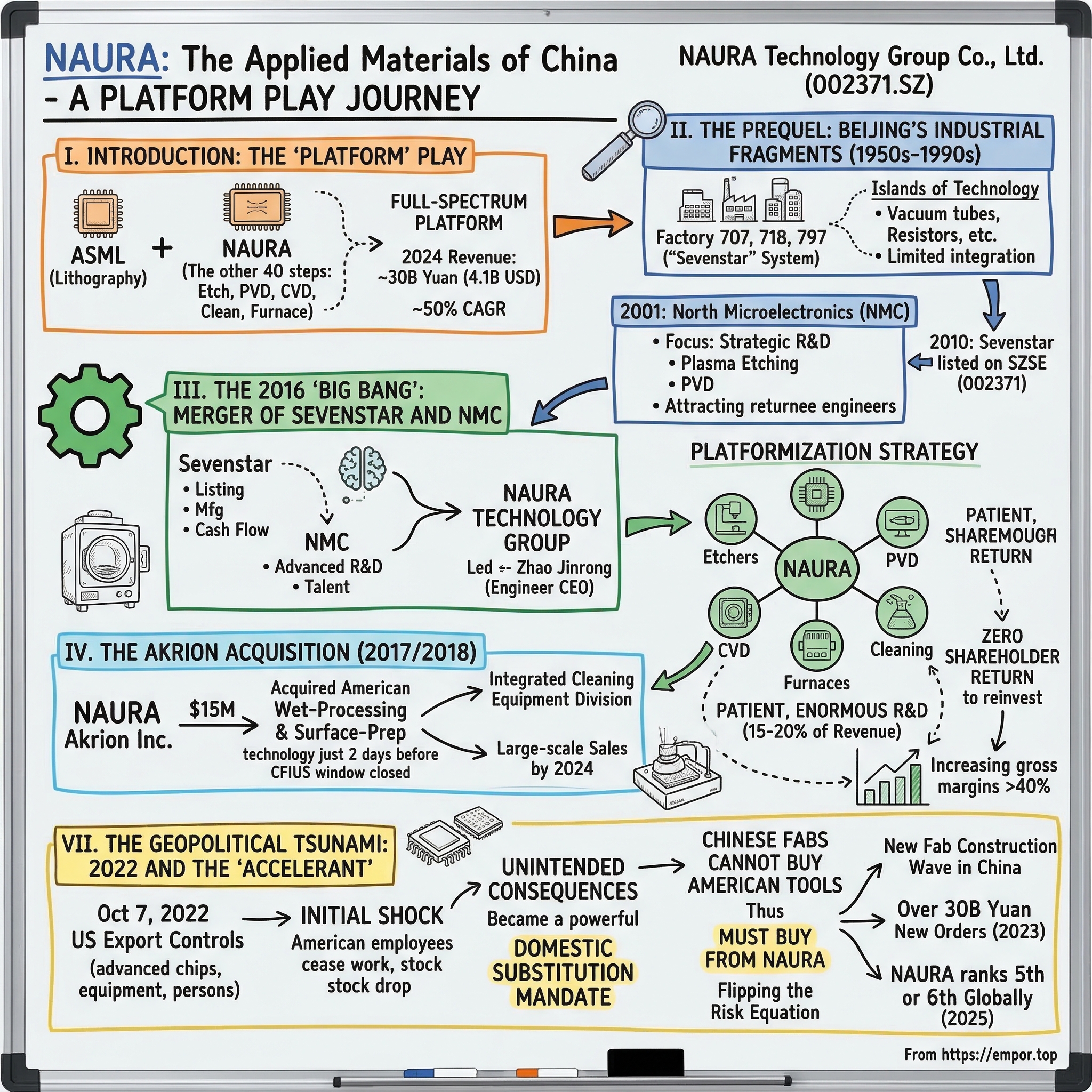
NAURA: The Applied Materials of China
I. Introduction: The "Platform" Play
In the global chip war, one machine has captured the world's imagination: the extreme ultraviolet lithography scanner built by ASML, the Dutch marvel that prints circuits at the atomic scale. Documentaries have been made about it. Export bans have been written around it. But here is a question that almost nobody outside the semiconductor industry asks: what happens after the lithography step?
The answer is: about forty other process steps, each requiring its own specialized, multi-million-dollar machine. After a pattern is printed onto a silicon wafer, that wafer must be etched — material chemically blasted away in precise nanometer-scale trenches. Then thin films of metal or insulator must be deposited, atom by atom, through processes called PVD and CVD. The wafer must be heated in furnaces to activate dopants. It must be cleaned, sometimes dozens of times, to remove particles that would kill a circuit. Each of these steps requires a different tool, and each tool represents a multi-billion-dollar global market.
For decades, three American and Japanese giants have owned these markets. Applied Materials, headquartered in Santa Clara, is the colossus — roughly $27 billion in annual revenue, building tools for deposition, etch, and inspection. Lam Research dominates plasma etch and deposition. Tokyo Electron covers coating, cleaning, and thermal processing. Together, these three companies, along with ASML and KLA, control over 80% of the global semiconductor equipment market. They are the picks-and-shovels suppliers to the $600 billion chip industry, and for a generation, no one has seriously challenged their oligopoly.
Until now. Buried in the industrial parks of Beijing's Yizhuang Economic Development Zone, a company called NAURA Technology Group has been quietly assembling something that no other Chinese firm has attempted: a full-spectrum semiconductor equipment platform. Not a single-product specialist. Not a niche player making one type of furnace. A company that builds etchers, PVD systems, CVD chambers, cleaning tools, diffusion furnaces, and rapid thermal processors — all under one roof. In 2024, NAURA posted revenue of nearly 30 billion yuan, roughly $4.1 billion, up from just 6 billion yuan four years earlier. That is a five-year compound annual growth rate approaching 50%. The company now ranks fifth or sixth among the world's semiconductor equipment makers, the only Chinese firm in the global top ten.
The thesis is straightforward but enormous in its implications. NAURA is running the Applied Materials playbook — becoming the one-stop shop that can outfit an entire semiconductor fabrication line — but doing it inside China, powered by a domestic substitution mandate that amounts to the largest forced technology transition in industrial history. Every Chinese fab that cannot buy American tools must now buy from NAURA. And there are a lot of Chinese fabs being built.
But the story is far more complex than "government money plus captive market equals success." To understand how NAURA arrived at this moment, you have to go back to a time when China's semiconductor equipment industry was not an industry at all — just a collection of scattered, state-owned fragments trying to make sense of a technology that was rapidly leaving them behind.
II. The Prequel: Beijing's Industrial Fragments
In the late 1950s, as the Cold War reshaped global technology, China established a series of state-owned electronics factories in Beijing, numbered in the 700-series and collectively known as the "Sevenstar" system. These were not semiconductor companies in any modern sense. They made vacuum tubes, basic resistors, crystal oscillators, and the kind of precision electronic components that a developing industrial economy needed for its military and telecommunications infrastructure. Factory 707, Factory 718, Factory 797 — each had a specialty, each reported to the Ministry of Electronics Industry, and each operated in near-total isolation from the global semiconductor revolution unfolding in Silicon Valley and later in Taiwan, South Korea, and Japan.
By the 1990s, these factories found themselves in a strange position. They possessed genuine expertise in vacuum technology, thermal processing, and precision manufacturing — skills that, in theory, were directly applicable to semiconductor equipment. But they had no integration, no system-level thinking, and no connection to the cutting-edge process nodes being developed by TSMC and Intel. China had what industry observers called "islands of technology" — isolated pockets of competence floating in a sea of irrelevance. The country could build a decent diffusion furnace for 6-inch wafers, but the world had moved to 8-inch and was racing toward 12-inch. The gap was not just wide; it was accelerating.
The turning point came in 2001. Beijing Electronics Holdings, the state entity that controlled the Sevenstar system, established a new subsidiary called North Microelectronics, or NMC. This was not another legacy factory repurposed with a new name. NMC was designed from scratch as a high-technology R&D organization focused on two of the most strategically important semiconductor process steps: plasma etching and physical vapor deposition. Think of it as a "Special Forces" unit — small, elite, technically ambitious, and specifically tasked with cracking the code of the tools that Applied Materials and Lam Research had spent decades perfecting.
NMC attracted a cadre of engineers, many of them returnees from overseas programs and universities, who understood what world-class semiconductor equipment looked like. They knew that building an etcher was not just an engineering problem but a materials science problem, a plasma physics problem, and a manufacturing precision problem all wrapped into one. The challenge was immense. A plasma etcher must generate and control ionized gas at temperatures and pressures that strip away material one atomic layer at a time, with uniformity across a 300-millimeter wafer that varies by less than a few percent. The chamber design, the gas chemistry, the RF power delivery, the electrostatic chuck that holds the wafer — every subsystem must work in concert at tolerances that border on the absurd.
NMC made progress. By the mid-2000s, it had prototype etchers and PVD tools running in Chinese fabs. But progress and commercial viability are different things. The global semiconductor equipment market operates on a brutal dynamic: fabs will not "qualify" a new tool unless it can demonstrate equivalent or superior performance to the incumbent, and qualification itself takes months or years of testing. Even if a NAURA etcher worked perfectly in a lab, convincing a fab manager to risk a billion-dollar production line on an unproven Chinese tool was nearly impossible. The installed base advantage of Applied and Lam was not just a market share number — it was encoded in decades of process recipes, service contracts, and institutional trust.
Meanwhile, across Beijing, the original Sevenstar entity was plodding along with its legacy businesses. It made diffusion furnaces, crystal growth equipment, gas mass flow controllers, and precision electronic components. The products were solid if unspectacular, and the company had achieved a milestone in March 2010 by listing on the Shenzhen Stock Exchange under ticker 002371 — the first Chinese integrated circuit equipment maker to go public. But Sevenstar was a small company in a giant's game, and NMC was a research outfit burning cash without a clear path to scale. By 2015, both entities faced the same existential question: in a global market dominated by American and Japanese companies spending billions on R&D, how does a Chinese equipment maker survive, let alone grow?
The answer, it turned out, was to stop being two companies and become one.
III. The 2016 "Big Bang": The Merger of Sevenstar and NMC
The merger was announced in 2016 and completed in early 2017, and the logic was almost painfully obvious in retrospect. Sevenstar had the public listing, the manufacturing infrastructure, the sales channels, and the steady cash flow from legacy businesses. NMC had the advanced R&D capabilities, the next-generation product pipeline, and the engineering talent. Apart, each was incomplete. Together, they could form something that China's semiconductor industry desperately needed: a platform company.
On February 24, 2017, the combined entity was officially renamed NAURA Technology Group Co., Ltd. The name itself was a statement of ambition — a clean break from the "Sevenstar" legacy, signaling that this was no longer a component maker but a technology group with aspirations to compete on the global stage. And the man chosen to lead it was Zhao Jinrong, the former president of NMC, the R&D side of the house. That choice told you everything about where the company intended to go. NAURA would be led by an engineer, not a bureaucrat.
The strategic vision crystallized around a concept borrowed directly from Applied Materials: platformization. In the semiconductor equipment industry, a platform company does not just make one type of tool. It makes etchers and depositors and furnaces and cleaners, and it sells them as an integrated package to fabs. The advantage is profound. A fab building a new production line needs dozens of different tools from multiple vendors, each with its own service contract, spare parts supply chain, and process integration requirements. A platform company can offer a bundled solution — fewer vendors to manage, integrated process recipes, and volume discounts that a single-product competitor cannot match. Applied Materials built its $27 billion empire on exactly this model.
But platformization requires something that most Chinese technology companies lacked: patient, sustained, enormous R&D investment. NAURA's leadership understood that they were not going to close a twenty-year technology gap by being incrementally better. They needed to outspend the incumbents as a percentage of revenue, even if their absolute R&D dollars remained a fraction of Applied's budget. And this is where the public listing became crucial.
Between 2017 and 2025, NAURA poured money into research at a rate that would make most Western semiconductor equipment companies blink. The company consistently spent between 15% and 20% of its revenue on R&D — in 2023, that meant roughly 4.8 billion yuan, or about $660 million. For comparison, Applied Materials spends about 15% of its much larger revenue base on R&D, but Applied is also returning billions to shareholders through buybacks and dividends. NAURA's "capital deployment" strategy is the exact opposite: almost zero return to shareholders, almost everything reinvested in closing the technology gap. It is, in effect, a ten-year, multi-billion-dollar bet on platformization, funded by the public markets and backstopped by the Chinese government's strategic priorities.
The results began to show in the product portfolio. By 2020, NAURA offered etchers covering processes from 90nm down to 28nm, with work underway on 14nm-capable tools. Its PVD systems were being adopted for metal interconnect layers. Its diffusion furnaces had evolved from legacy 6-inch tools to modern 12-inch systems capable of advanced oxidation, annealing, and low-pressure chemical vapor deposition. The company launched PECVD tools, atomic layer deposition furnaces, rapid thermal processing systems, and a growing suite of cleaning equipment. Each new product line did not just add revenue — it added another piece to the platform puzzle, making NAURA incrementally more attractive to fabs that wanted to consolidate their vendor base.
The financial trajectory told the story in stark terms. Revenue doubled from 6 billion yuan in 2020 to nearly 10 billion in 2021, then doubled again to almost 15 billion in 2022. Gross margins, which had hovered in the mid-30s during the pre-merger Sevenstar era, climbed above 40% as the higher-value semiconductor equipment segment grew to dominate the revenue mix. NAURA was not just getting bigger; it was getting more profitable as its platform strategy created the kind of operating leverage that only comes from spreading fixed R&D costs across a widening product portfolio. The very dynamic that had made Applied Materials a $150 billion market cap company was beginning to work for NAURA — at smaller scale, in a protected market, but with growth rates that the American giant had not seen in decades.
IV. The Akrion Acquisition and the M&A Playbook
In the summer of 2017, NAURA's leadership made a decision that, in retrospect, looks like one of the shrewdest moves in the entire Chinese semiconductor equipment industry. They announced the acquisition of Akrion Systems, a small, Pennsylvania-based company that made wet-processing and surface-preparation equipment for semiconductor fabs. The price was approximately $15 million.
Fifteen million dollars. In an industry where a single EUV lithography scanner costs $380 million, NAURA paid less than the price of a modest office building in Palo Alto for an entire company with proprietary cleaning technology, an installed base of customers, and — critically — a team of American engineers who understood how to build semiconductor-grade wet processing tools.
Akrion was not a household name. Headquartered in Allentown, Pennsylvania, it specialized in the machines that clean silicon wafers between process steps — removing particles, residues, and contaminants that could destroy circuit yields. Wafer cleaning is one of the most frequently performed steps in semiconductor manufacturing. A wafer might go through dozens of cleaning cycles during its journey through a fab, and each cycle requires precisely controlled chemistry, temperature, and mechanical action. Akrion had built a solid business serving both the semiconductor and photovoltaic industries, but it was small, subscale, and struggling to compete against the cleaning divisions of much larger companies like Screen Holdings and Lam Research.
For NAURA, the acquisition was a technology accelerant. Building cleaning equipment from scratch would have taken years of development, qualification, and iteration. By acquiring Akrion, NAURA got a running start — proven designs, established process recipes, and the kind of institutional knowledge that cannot be replicated by reading patents. The deal was executed through a newly formed U.S. subsidiary called NAURA Akrion Inc., and it closed on January 16, 2018.
But the timing of this deal is what elevates it from clever to historic. On January 18, 2018 — just two days after closing — NAURA received clearance from CFIUS, the Committee on Foreign Investment in the United States, which reviews foreign acquisitions for national security implications. This was, remarkably, the first acquisition of a U.S. semiconductor company by a Chinese buyer to be approved after Donald Trump took office. The political winds were already shifting. Within months, the trade war between the United States and China would escalate dramatically. Within a few years, CFIUS reviews of Chinese acquisitions in the semiconductor space would become so restrictive as to be effectively prohibitive.
NAURA had slipped through a window that was closing fast — and everyone involved knew it. The $15 million price tag, in this context, was not just a bargain. It was the last ticket on a train that would never run again. Every subsequent Chinese attempt to acquire American semiconductor technology through M&A has faced either CFIUS rejection or such intense scrutiny that deals collapse before they reach the finish line. NAURA's Akrion deal stands as one of the final successful cross-border semiconductor acquisitions of the pre-decoupling era.
The Akrion technology was integrated into NAURA's cleaning equipment division, and by 2024, the company reported that its stacked wafer cleaning systems had achieved "large-scale sales" — industry language meaning they had moved from qualification to volume production in multiple customer fabs. The $15 million investment had seeded an entire product line that now contributes meaningfully to the platform strategy. In an industry where R&D programs routinely consume hundreds of millions of dollars before producing a single commercial tool, the Akrion acquisition was dollar-for-dollar one of the highest-return M&A deals in semiconductor equipment history.
V. Management and the "Professionalized" State Enterprise
There is a default narrative about Chinese state-linked enterprises that goes something like this: they are bureaucratic, politically driven, technically mediocre, and more interested in meeting five-year-plan targets than in building world-class products. For some companies, this narrative is accurate. For NAURA, it is almost entirely wrong, and the reasons why tell you something important about how the best Chinese technology companies actually operate.
Start with the man at the top. Zhao Jinrong became chairman of NAURA after the 2017 merger, having previously led NMC, the R&D-focused subsidiary. Zhao is not a politician who was assigned to run a technology company. He is an engineer who rose through the ranks of one of China's most technically demanding organizations. His background is in semiconductor process technology, and his career has been defined by the unglamorous, intensely difficult work of building tools that can deposit metal films at angstrom-level precision or etch trenches with vertical sidewalls at the 14nm node. In 2022, Zhao received the Zhongguancun Award for Outstanding Contributions — Beijing's top science and technology recognition, the Chinese equivalent of being named to the National Academy of Engineering.
Zhao's leadership style is what you might call "technocratic operational" — less the charismatic founder-visionary of Silicon Valley mythology and more the disciplined engineering executive who builds systems, processes, and teams. Under his direction, NAURA has adopted what employees describe as a "Huawei-style" culture: long hours, intense technical scrutiny, rapid iteration cycles, and a meritocratic promotion system that rewards engineering achievement over political connections. This is not the sleepy state-owned enterprise of Western imagination. It is, by most accounts, one of the most demanding workplaces in China's technology sector.
But culture alone does not explain NAURA's ability to attract and retain the caliber of engineers needed to build semiconductor equipment. The real innovation is in the incentive structure. Despite its state-linked ownership — Beijing Electronics Holdings remains a significant shareholder — NAURA has implemented some of the most aggressive equity incentive plans in China's technology sector.
The 2019 Stock Option Incentive Plan issued approximately 4.5 million stock options and 4.5 million restricted shares, covering 88 senior managers and 354 core technical and management personnel. The stock option exercise price was set at 69.2 yuan per share, and the restricted stock grant price at 34.6 yuan — both well below the market price at the time of vesting, creating significant wealth for participants as NAURA's stock surged. The company followed this with additional plans in 2024 and 2025, including a 2025-2027 Employee Stock Ownership Plan that extends equity participation even further down the organization.
The numbers matter. Over 2,000 "key technical staff" across the company now have meaningful equity exposure. In a country where semiconductor engineers are in ferocious demand — poached by rival firms, lured by startups, recruited by provincial governments offering lavish relocation packages — NAURA's ability to retain its engineering core is a competitive advantage that does not show up on any balance sheet. The implicit bargain is clear: stay, build great tools, and the equity will make you wealthy. Leave, and you walk away from unvested options tied to aggressive revenue and R&D milestones.
This structure also addresses one of the deepest skepticisms that foreign investors hold about Chinese state-linked companies: agency risk. When management has no personal financial stake in outcomes, the risk of empire-building, political allocation of capital, and indifference to returns is high. NAURA's equity plans do not eliminate this risk — the company is still subject to government policy priorities and state-directed capital allocation — but they meaningfully align management's economic interests with shareholder value creation. It is not Silicon Valley governance. But it is a long way from the stereotypical SOE.
In March 2026, Zhao co-authored a public call with other leading semiconductor industry figures for a coordinated national effort to develop lithography systems during the 2026-2030 period — an initiative aimed at creating "China's ASML." The move signaled both the extent of Zhao's influence within the Chinese semiconductor policy establishment and the scale of NAURA's ambitions. The company is no longer content to be the platform provider for everything except lithography. It wants the whole cleanroom.
VI. Hidden Engines: The "Other" NAURA
When analysts and investors discuss NAURA, the conversation almost invariably centers on semiconductor equipment — and for good reason. The semiconductor segment now generates roughly 80% of total revenue and is growing faster than any other part of the business. But to understand NAURA's full economic engine, and to appreciate the strategic optionality embedded in its platform, you need to look at the parts of the company that rarely make headlines.
NAURA operates three reportable segments. The first and largest is semiconductor equipment, which covers everything from etchers and PVD systems to furnaces, cleaning tools, and the growing suite of deposition technologies. In fiscal 2024, this segment generated over 21 billion yuan in revenue, and in the first half of 2025 alone, it exceeded 13 billion yuan. The growth here is driven by the domestic substitution wave — Chinese fabs building new capacity and, increasingly, replacing Western tools with domestic alternatives. This is the segment that gets NAURA compared to Applied Materials, and it is the segment that will determine whether the company becomes a global top-three player or plateaus as a regional champion.
The second segment is vacuum and new energy equipment, and this is where the hidden story lies. NAURA's core competencies — vacuum engineering, thermal processing, precision gas control — are not specific to semiconductors. They apply to any industry that requires controlled-atmosphere, high-temperature processing of materials. This means aerospace components that must be heat-treated in vacuum to achieve specific metallurgical properties. It means crystal growth equipment for the silicon ingots used in solar panels. It means furnaces for processing the magnetic materials used in electric vehicle motors. And, increasingly, it means equipment for lithium battery production — the mixers, coaters, and winders that form the backbone of EV battery manufacturing lines.
This is not a trivial sidecar business. The vacuum and new energy segment leverages exactly the same engineering disciplines that NAURA has built for semiconductor equipment, but serves markets with different growth drivers and different competitive dynamics. The global lithium battery equipment market is growing at double-digit rates as EV adoption accelerates worldwide, and Chinese manufacturers dominate global battery production. NAURA's ability to provide high-end vacuum furnaces and thermal processing equipment to battery makers like CATL and BYD creates a revenue stream that is partially decoupled from the cyclical semiconductor capex cycle. When chip spending softens — as it periodically does — battery equipment spending may continue to grow, and vice versa.
The synergy between semiconductor and vacuum equipment is real but subtle. The engineering challenge of building a diffusion furnace that can uniformly heat 150 silicon wafers to 1,200 degrees Celsius in a controlled gas environment is nearly identical to the challenge of building a vacuum furnace that can heat-treat a turbine blade for a jet engine. The materials are different, the process recipes are different, but the underlying physics — heat transfer, gas dynamics, vacuum integrity, contamination control — is the same. Engineers who solve problems in one domain develop intuitions and techniques that transfer directly to the other. This cross-pollination of expertise is a form of invisible competitive advantage that NAURA's structure enables.
The third segment, precision electronic components, is the oldest part of the business — the direct descendant of those 700-series factories from the 1950s. It makes resistors, capacitors, crystal oscillators, microwave components, and power supply modules, primarily for aerospace, defense, and industrial applications. The revenue contribution is relatively small and the growth modest, but the strategic role is important. This is the "boring" cash cow that threw off steady profits during the years when the semiconductor equipment division was consuming capital and posting losses. In the early days of NAURA's platform buildout, the components business provided the financial cushion that allowed the company to take risks on unproven semiconductor tools without facing an existential cash crunch. Every great technology company needs a cash-flow anchor during its high-investment phase, and for NAURA, precision components played that role.
Looking at the consolidated picture, what emerges is a company with more strategic depth than its headline semiconductor equipment numbers suggest. The vacuum and energy business provides diversification and leverages core competencies into adjacent high-growth markets. The components business provides stability and cash flow. And the semiconductor equipment business provides the growth engine and the narrative that justifies a premium valuation. It is a surprisingly well-balanced portfolio for a company that most people think of as a pure-play semiconductor equipment maker — and it is a portfolio that becomes more valuable, not less, as NAURA's core engineering capabilities compound over time.
VII. The Geopolitical Tsunami: 2022 and the "Accelerant"
October 7, 2022, is a date that will be studied in business schools and policy institutes for decades. On that day, the U.S. Bureau of Industry and Security published a sweeping set of export controls targeting China's semiconductor industry — the most significant technology restriction since the Cold War. The controls went far beyond previous measures. They restricted the sale of advanced semiconductor manufacturing equipment to China, barred American citizens and permanent residents from working in Chinese chip fabs, and created new licensing requirements for a wide range of tools and components that had previously flowed freely across the Pacific.
The stated goal was to prevent China from manufacturing advanced chips — specifically, logic chips at the 14nm node and below, and advanced memory chips — that could be used in artificial intelligence, supercomputing, and military applications. The practical effect was to throw a wrench into the supply chains of every Chinese semiconductor manufacturer and, simultaneously, to create the most powerful domestic substitution mandate in the history of industrial policy.
For NAURA, the initial impact was jarring. The company instructed its American employees working in China to immediately cease participation in R&D activities, complying with the new rules that prohibited "U.S. persons" from supporting Chinese semiconductor manufacturing. NAURA's subsidiary, Beijing Naura Magnetoelectric Technology, was placed on the Bureau of Industry and Security's Unverified List — a designation that, while short of the more severe Entity List, signaled heightened scrutiny and complicated the company's ability to procure certain U.S.-origin components. The stock dropped 20% in the week following the announcement. Yangtze Memory Technologies Corp, or YMTC, one of NAURA's largest customers, slashed equipment purchase orders by 70% in early 2023 as it scrambled to assess the impact of being directly targeted by the new controls.
But within months, a paradox emerged that perfectly illustrated the law of unintended consequences. The same export controls that were supposed to slow China's chip industry became the most effective sales force NAURA had ever had.
The logic was inescapable. Before October 7th, a Chinese fab building a new 28nm production line had a choice: buy proven, best-in-class tools from Applied Materials and Lam Research, or take a risk on less-established domestic alternatives from NAURA and AMEC. Most chose the American and Japanese tools. The performance was better, the process recipes were more mature, the service infrastructure was deeper, and qualification risk was lower. NAURA was a "nice-to-have" — a patriotic option, a hedge against supply disruption, but not the first call.
After October 7th, the calculus inverted. Chinese fabs could no longer guarantee that they would be able to buy American tools, or that tools they had already ordered would be delivered, or that spare parts and service for installed American equipment would continue to be available. The risk equation flipped: now it was the American tools that carried supply risk, and the domestic tools that offered certainty. Overnight, NAURA went from "domestic alternative" to "national security mandate."
The revenue surge was immediate and dramatic. In 2023, NAURA received over 30 billion yuan in new equipment orders, with more than 70% destined for semiconductor manufacturing. Full-year revenue hit 22 billion yuan, up 50% from the prior year. In 2024, revenue climbed to nearly 30 billion yuan. By the first half of 2025, the pace showed no signs of slowing. The company's order backlog — a leading indicator of future revenue — swelled to levels that implied years of production ahead.
But the demand surge was not just about fear and supply security. The export controls also triggered an unprecedented wave of new fab construction across China. Paradoxically, by trying to limit China's access to advanced chipmaking tools, the U.S. controls motivated the Chinese government and private sector to double down on semiconductor investment. Provincial governments competed to attract new fabs. The National IC Investment Fund, China's multi-billion-dollar semiconductor war chest, accelerated capital deployment. SMIC, Hua Hong, and other Chinese foundries announced expansion after expansion, primarily at the mature nodes — 28nm and above — that were not directly restricted but where domestic tool qualification was most advanced.
Each new fab needed a full complement of equipment, and NAURA's platform breadth meant it could supply multiple tool types to each facility. A new 28nm production line might require NAURA etchers, NAURA PVD systems, NAURA furnaces, and NAURA cleaning tools — a bundled purchase that no other Chinese equipment company could offer. The platform strategy that Zhao Jinrong had been building since 2017 was suddenly not just a competitive advantage but a near-monopolistic one in the context of a domestic market that had few other places to turn.
By late 2025, industry analysts estimated that China's semiconductor equipment self-sufficiency rate had approached 50%, up from roughly 15-20% before the export controls. NAURA was the single largest beneficiary of this shift. The company climbed from eighth in global semiconductor equipment rankings in 2022 to fifth or sixth by 2025 — leapfrogging European and Japanese competitors who had spent decades building their positions. Three Chinese firms, including NAURA, entered the world's top twenty semiconductor equipment companies for the first time. The geopolitical tsunami that was supposed to sink China's chip ambitions had, instead, created the conditions for the fastest equipment market share shift in the industry's history.
VIII. The Playbook: 7 Powers and Porter's 5 Forces
To evaluate NAURA as a long-term investment, it helps to step back from the quarterly revenue numbers and ask a more fundamental question: what are the structural sources of competitive advantage that protect this company's position and allow it to earn returns above its cost of capital?
Hamilton Helmer's Seven Powers framework provides a useful lens. The most powerful and unusual advantage NAURA possesses is what Helmer would call a Cornered Resource — except in this case, the resource is not a patent or a genius founder but an entire regulatory regime. The Chinese government's domestic substitution mandate is, in effect, a moat that no Western competitor can cross. Applied Materials cannot build a fab in China and sell tools domestically to circumvent export controls. Lam Research cannot lobby Beijing for equal treatment. The policy environment creates a captive market of enormous and growing size, and NAURA — as the broadest domestic platform — is the primary beneficiary. This is not a moat built on technological superiority. It is a moat built on geopolitics, and it is arguably more durable than any technology advantage because it is reinforced by the self-interest of a sovereign government that views semiconductor independence as a matter of national security.
The second power is Scale Economies, and here the platform strategy becomes central. Every new product line that NAURA adds to its portfolio does two things: it spreads fixed R&D costs across a larger revenue base, and it increases the company's "bundling" power at the fab level. A Chinese fab that already uses NAURA etchers has a strong incentive to evaluate NAURA's PVD tools for the next expansion, because a single vendor relationship reduces procurement complexity, simplifies process integration, and provides negotiating leverage. As NAURA moves from three or four product categories to eight or ten, this bundling dynamic compounds. The R&D cost per incremental tool type declines because many of the underlying engineering disciplines — vacuum systems, plasma physics, gas delivery, contamination control — are shared across products. This is the same dynamic that made Applied Materials the most profitable semiconductor equipment company in the world, and NAURA is replicating it at an accelerated pace.
The third power is Switching Costs, and in semiconductor equipment, these are among the highest of any industry. When a NAURA etcher is "qualified" into a production process — say, a 28nm logic line at SMIC — it becomes embedded in the fab's process recipe. The etch parameters, the gas mixtures, the chamber conditioning procedures, and the defect specifications are all calibrated to that specific tool. Swapping it out for a competitor's etcher would require months of re-qualification, yield risk, and process re-optimization. In practice, once a tool is qualified, it stays in the line for a decade or more. This creates an annuity stream of spare parts, consumables, and service revenue that flows long after the initial tool sale, and it raises an almost prohibitive barrier to competitive displacement.
Porter's Five Forces analysis reinforces and extends these structural observations. The bargaining power of buyers — Chinese semiconductor fabs — is paradoxically low despite their size and strategic importance. In a market where domestic alternatives are limited, NAURA faces fewer price-pressure dynamics than a Western equipment company selling into a competitive global market. Chinese fabs need NAURA's tools, and there is no credible second source for most of the product categories where NAURA has qualified into production. The bargaining power of suppliers is moderate; NAURA still depends on certain imported components, particularly for precision subsystems and some electronic controls, though the company has been aggressively localizing its supply chain.
The threat of new entrants is real but contained. China's semiconductor equipment industry includes other capable companies — AMEC in etch, ACM Research in cleaning, Piotech in deposition — but none has attempted NAURA's platform breadth. Building a platform company from scratch would require a decade of investment and a willingness to sustain losses across multiple product lines simultaneously, which is why NAURA's head start is so valuable. AMEC, the most frequently cited competitor, is a specialist etch company with perhaps a quarter of NAURA's revenue. Its CCP etch tools are reportedly used in some 5nm production lines, making it arguably more advanced than NAURA in that specific niche. But AMEC does not make PVD systems, or furnaces, or cleaning tools. It is a single-product champion competing against a multi-product platform, and the platform advantages compound over time.
The competitive rivalry is intense at the local level but fundamentally different from global competition. NAURA and AMEC are not fighting over the same fab dollar the way Applied and Lam fight over TSMC's capex budget. They are fighting over adjacent product categories in a domestic market that is growing fast enough to accommodate both. The real competitive question is whether NAURA can maintain its platform lead as other Chinese companies mature and whether it can extend its capabilities to more advanced nodes — 7nm, 5nm, and below — where the technology challenges are exponentially harder.
The threat of substitutes is minimal. There is no alternative to semiconductor manufacturing equipment for making semiconductors. Until someone invents a fundamentally different way to build chips — and no one has — the tools that etch, deposit, clean, and heat silicon wafers will remain indispensable.
IX. Bear vs. Bull Case
Every investment has a story, and the most useful exercise for any long-term investor is to stress-test that story against its strongest opposing narrative. NAURA's story is powerful — a platform company riding a once-in-a-generation domestic substitution wave in the world's fastest-growing semiconductor market. But powerful stories are exactly the ones that deserve the most rigorous scrutiny.
The bear case begins with technology. NAURA's tools are primarily qualified at mature process nodes — 28nm and above for most products, with some capabilities extending to 14nm. The company has made progress on more advanced nodes, but the gap between 14nm-capable and 5nm-capable is not linear. It is exponential. At advanced nodes, the precision requirements for etch uniformity, film thickness control, and contamination management increase by orders of magnitude. The physics change. New materials — cobalt instead of copper for interconnects, hafnium oxide for gate dielectrics, extreme ultraviolet-sensitive photoresists — require entirely new tool designs and process chemistries.
The bear asks: can NAURA make this leap without access to certain Western sub-components and know-how? The company still depends on some imported precision parts — specialized RF generators, certain vacuum pumps, advanced metrology sensors — that may be subject to future export restrictions. If the U.S. tightens controls further, NAURA's ability to push into advanced nodes could be constrained not by its own engineering capability but by its supply chain. The Akrion-style M&A window is closed. The talent pipeline from Western companies has been disrupted. The path to the bleeding edge is narrow and uncertain.
The bear case also raises the "jack of all trades, master of none" concern. NAURA's platform breadth is a strength in bundling and customer convenience, but it also means the company is spreading its R&D resources across many product categories simultaneously. AMEC, by contrast, can concentrate all of its engineering talent on etch, and in that single category, it appears to be ahead of NAURA in node capability. If each of NAURA's product lines is "good enough" for domestic fabs but never quite world-class, the company might find itself stuck in a middle ground — too broad to be the best at anything, too dependent on policy protection to compete globally.
There is also the question of what happens if geopolitical tensions ease. If, hypothetically, U.S.-China trade relations improve and export controls are relaxed, Chinese fabs would once again have the option to buy American tools. Would they? The switching costs discussed earlier suggest that qualified NAURA tools would remain in place, but for new fab lines and expansions, some customers might revert to the higher-performance Western incumbents. The domestic substitution mandate is durable — but it is not guaranteed to be permanent.
The bull case starts with the simplest and most powerful observation: if China builds chips, NAURA wins. This is not a company that needs to convince customers to adopt a new technology or change their behavior. The demand is structural and mandated by national policy. China has committed to spending hundreds of billions of dollars on semiconductor manufacturing capacity over the next decade, and a significant and growing share of the equipment for that capacity will be sourced domestically. NAURA, as the only platform-type equipment company in China, is the toll booth on this highway.
The bull points to the revenue trajectory — from 6 billion yuan in 2020 to nearly 30 billion in 2024, with forecasts suggesting 47-52 billion in 2025 — and argues that this is not a peak. China's semiconductor equipment self-sufficiency is approaching 50%, but that means half the market is still served by foreign tools that are increasingly unreliable to supply. The runway for domestic substitution extends for years, possibly decades. And each incremental percentage point of market share gained by NAURA comes at improving margins, because the fixed R&D investments have already been made and the incremental cost of producing additional tools is primarily variable.
The bull also emphasizes NAURA's expanding ambitions. The 2025 acquisition of a controlling stake in Shenyang Piotech added CVD and ALD deposition capabilities — two of the fastest-growing tool categories in advanced semiconductor manufacturing. The investment in Kingsemi, with plans to acquire a controlling stake, brings NAURA into the coating and developing track equipment market — the photolithography-adjacent tools that complement the exposure step. And Zhao Jinrong's public advocacy for a national lithography development program signals that NAURA may eventually attempt the most ambitious expansion of all: building China's alternative to ASML's scanners. Whether or not NAURA succeeds at lithography, the intent demonstrates a management team that is thinking in decades, not quarters.
For investors tracking NAURA's ongoing performance, two KPIs stand above the rest. The first is the domestic semiconductor equipment substitution rate — the share of equipment in Chinese fabs that is sourced from Chinese suppliers. This is the single most important macro indicator for NAURA's addressable market. As this rate climbs from 50% toward 70% or beyond, NAURA's revenue has an almost mechanical tailwind. The second KPI is R&D spending as a percentage of revenue. This metric tells you whether management is maintaining the investment intensity needed to close the technology gap with Applied Materials and Lam Research. If R&D intensity drops below 12-13% for sustained periods, it may signal that the company is prioritizing short-term profitability over long-term competitiveness — a warning sign in an industry where the technology frontier moves relentlessly forward.
What NAURA represents, ultimately, is not just a company but a twenty-year national project to build a sovereign semiconductor equipment industry. The question is not whether this project will produce results — it already has. The question is whether those results can compound from "good enough for mature nodes in a protected market" to "competitive at advanced nodes on the global stage." The answer to that question will determine whether NAURA's current trajectory leads to a $100 billion company or a $20 billion one, and it will depend on factors — geopolitical, technological, and organizational — that no financial model can fully capture.
X. Outro and Key Links
The story of NAURA Technology Group is, in many ways, the story of China's broader semiconductor ambitions distilled into a single company. From the scattered fragments of 1950s-era state factories to a $4 billion platform company ranked among the world's top five equipment makers, NAURA's trajectory traces the arc of a nation that decided — belatedly, expensively, but with extraordinary determination — that it would build its own semiconductor supply chain, no matter the cost.
For readers who want to go deeper, Chris Miller's "Chip War: The Fight for the World's Most Critical Technology" provides the definitive account of how the global semiconductor industry became the centerpiece of great-power competition. Miller's treatment of the equipment supply chain — and the strategic chokepoints that companies like ASML, Applied Materials, and now NAURA occupy — is essential context for understanding why a company that makes etchers and furnaces sits at the nexus of the most consequential technology competition of the 21st century.
For the technically inclined, it is worth understanding the distinction between the two main categories of thin-film deposition that define much of NAURA's semiconductor product line. Physical vapor deposition, or PVD, works by physically dislodging atoms from a target material — usually by bombarding it with ionized argon gas — and letting those atoms settle onto the wafer surface to form a thin film. It is fast, produces dense films, and is the standard method for depositing metal layers like aluminum and copper interconnects. Chemical vapor deposition, or CVD, works differently: gaseous precursors are introduced into a heated chamber, where they react on the wafer surface to form a solid film. CVD is more versatile — it can deposit a wider range of materials, including insulators and semiconductors — but is generally slower and requires more complex chemistry. PECVD, plasma-enhanced CVD, uses plasma energy to drive the chemical reactions at lower temperatures, enabling deposition on temperature-sensitive substrates. ALD, atomic layer deposition, takes CVD to its logical extreme: depositing films one atomic layer at a time, achieving angstrom-level thickness control that is essential for the gate oxides and spacers in sub-10nm transistors. NAURA now has product lines in all four of these categories, a breadth that is unique among Chinese equipment makers.
The Applied Materials comparison that gives this episode its title is both apt and aspirational. Applied built its platform over four decades, through organic R&D and dozens of acquisitions, in the most favorable competitive environment imaginable — a growing global market with deep capital markets and unfettered access to the world's best engineering talent. NAURA is attempting to replicate that platform in a fraction of the time, in a constrained geopolitical environment, with a supply chain that is being deliberately severed from the Western ecosystem. That it has come as far as it has is remarkable. Whether it can go the rest of the way is the defining question for the company, for China's semiconductor industry, and — in no small measure — for the global technology order that will take shape over the coming decade.
 RSS Feed
 Spotify
 Apple Podcasts
 Amazon Music
 Audible
 YouTube