SK hynix: The AI Kingmaker
I. The Cold Open: March 2024
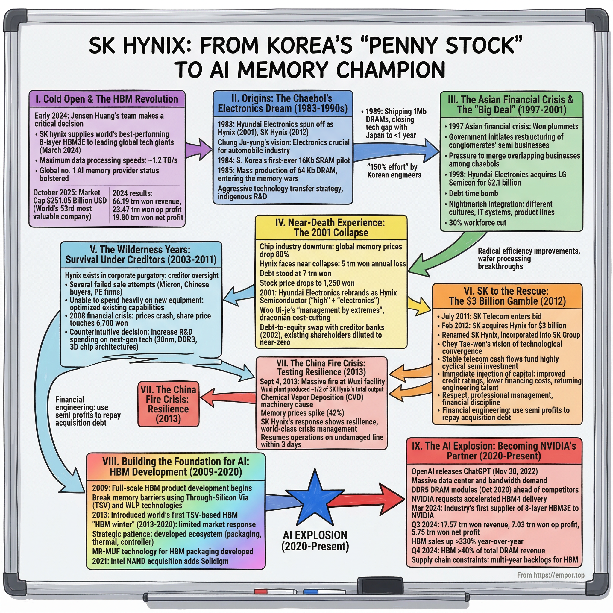
Picture this: the Jacob Javits Center in San Jose, March 2024, NVIDIA's GPU Technology Conference. The floor is buzzing with the usual suspects—cloud hyperscalers, AI startup founders, and chip engineers—all orbiting the gravitational pull of Jensen Huang. But on this particular day, the man in the black leather jacket does something unusual. He makes a beeline for a booth that, in prior years, might have been an afterthought—SK hynix. He picks up a wafer, signs it with a flourish, and poses for photos with the SK hynix team like they are old war buddies reuniting after a campaign. Because, in a very real sense, they are.
The moment was not just a photo op. It was a coronation. Jensen Huang, the most powerful figure in the semiconductor universe, was publicly acknowledging that the AI revolution does not run on GPUs alone. It runs on memory. Specifically, it runs on High Bandwidth Memory—HBM—and the company that makes most of the world's supply is SK hynix. Not Intel. Not Samsung. Not Micron. A company that, just two decades earlier, was a "zombie firm" under creditor control, hemorrhaging cash, and trading at valuations that would make a penny stock blush.
The stakes of this story are enormous. Every NVIDIA H100 GPU—the chip that powered the ChatGPT revolution—contains multiple stacks of HBM3 memory, almost all of it manufactured by SK hynix. Every B200, the next-generation chip powering the next wave of AI infrastructure, depends on HBM3E, where SK hynix again holds the dominant position. If TSMC is the foundry that fabricates Jensen's dreams, SK hynix is the memory that gives those dreams the bandwidth to think. Without it, the most advanced AI chips in the world are just very expensive paperweights.
But here is what makes this story truly extraordinary. SK hynix did not stumble into this position by accident, nor did it ride a lucky wave. This is a company that began developing stacked memory technology in 2009—a full fifteen years before the world decided it needed it. A company that survived three near-death experiences. A company whose engineers, working under creditor-imposed austerity, innovated their way out of oblivion while their larger, richer rival Samsung poured billions into staying ahead.
This is not just a story about chips. It is a story about what happens when patient capital meets relentless engineering. When a company forged in crisis builds the exact technology the future demands. When the most important company in the AI era turns out to be located not in Silicon Valley, not in Taipei, but in a small city called Icheon, nestled in the hills of Gyeonggi Province, South Korea.
II. The Origins: From Hyundai to "Hynix"
To understand SK hynix, you have to understand the peculiar alchemy of Korean industrial policy, chaebol ambition, and the brutal economics of memory semiconductors. The company that would eventually become SK hynix was born in 1983 as Hyundai Electronics, a division of the Hyundai Group—the same conglomerate that built ships, cars, and apartment towers. Chung Ju-yung, the legendary Hyundai founder, believed semiconductors would become as essential to Korea's future as steel and shipbuilding had been to its past. He was right, but the road would be far more punishing than anyone imagined.
Through the 1980s and early 1990s, Hyundai Electronics grew into a respectable DRAM manufacturer, riding the global PC boom. Memory chips are, at their core, a volume game—build the biggest fabs, achieve the best yields, and sell at prices that crush your competitors. It is a business where the learning curve is steep, capital requirements are enormous, and the cycle between boom and bust can be merciless. Hyundai played this game well enough to become a top-five global DRAM producer by the mid-1990s.
Then came 1997, and the Asian Financial Crisis detonated like a bomb across the Korean economy. The IMF bailout imposed harsh restructuring requirements on Korea's chaebols. The government, desperate to rationalize overlapping industries, mandated a series of "Big Deals"—forced mergers between competing chaebol units. In this environment, Hyundai Electronics was told to absorb LG Semicon, LG Group's semiconductor arm, in a deal valued at approximately two billion dollars. The merger, completed in July 1999, created a combined entity that was the world's second-largest DRAM maker. On paper, it looked like consolidation. In reality, it was two drowning companies lashed together.
The timing could not have been worse. The dot-com bubble burst in 2000, and by 2001, global DRAM prices had collapsed by roughly eighty percent. Hyundai Electronics, now saddled with billions in debt from the LG Semicon acquisition, was bleeding out. In 2001, the company recorded sales of four trillion won but losses of five trillion won, with total debt exceeding seven trillion won. The parent Hyundai Group, itself fracturing into pieces under the weight of the crisis, effectively abandoned its electronics subsidiary.
What followed was corporate triage on a massive scale. The company was rebranded as "Hynix Semiconductor" in 2001—a portmanteau meant to signal a fresh start, shedding the Hyundai name. Creditor banks, led by Korea Development Bank, took control through a debt-to-equity swap. Non-core businesses were divested: mobile phones, car navigation systems, flat-panel displays—anything that could be sold was sold. Hynix entered what Korean corporate culture euphemistically calls a "workout"—essentially, debtor-in-possession financing managed by bankers, not engineers.
But here is the part of the story that most analysts miss. The near-death experience did not break Hynix's engineering culture—it tempered it. With virtually zero discretionary budget, Hynix engineers were forced to innovate asymmetrically. They could not outspend Samsung. They could not match Samsung's fab capacity. So they had to outthink Samsung. This culture of resourcefulness, of finding the clever solution rather than the expensive one, became the "Golden Thread" that would eventually lead to HBM. As early as 2009, a small team at Hynix began experimenting with through-silicon vias (TSVs)—a technology for stacking memory chips vertically—not because anyone was asking for it, but because they believed it represented the future of memory bandwidth.
The creditor control era, which lasted roughly a decade, was miserable by any business school standard. But it produced something valuable: a workforce that knew how to survive anything. Engineers who had watched their company nearly die—not once, but repeatedly—developed a resilience and urgency that money cannot buy. They graduated from the workout program within approximately three years of entering it, a remarkably fast turnaround. But the stigma lingered. Hynix was still "the troubled one," the company that might not make it. What it needed was a patron with deep pockets, long time horizons, and the conviction to bet big on a business that the market had written off.
III. The 2012 Inflection Point: The SK Acquisition
In February 2012, SK Telecom—the wireless arm of SK Group, one of Korea's largest chaebols—announced it would acquire a 21.05 percent controlling stake in Hynix from creditor banks for 3.37 trillion won, approximately three billion dollars. The market reaction was, to put it charitably, skeptical. SK Group was known for energy and telecommunications, not semiconductors. Analysts questioned whether Chairman Chey Tae-won was making a vanity purchase, diversifying into a notoriously cyclical commodity business that had already humbled some of the world's largest companies.
Chey Tae-won is one of the more complicated figures in Korean business. The grandson of SK Group's founder, he took the helm of the conglomerate and transformed it from a regional textiles-and-oil company into a diversified technology powerhouse. He is also a man who served time in prison for embezzlement—twice—and was pardoned—twice—in a pattern that says as much about Korean corporate governance as it does about his personal story. But whatever his legal troubles, Chey's instinct for capital allocation has proven extraordinary. The Hynix acquisition stands as Exhibit A.
What made the deal brilliant was not just the price—though three billion dollars for what would become a nearly five-hundred-billion-dollar company is, in hindsight, almost comically cheap. What made it brilliant was the strategic clarity that Chey brought. He understood that memory semiconductors, despite their cyclical reputation, were entering a structural growth phase driven by smartphones, cloud computing, and eventually artificial intelligence. He also understood that Hynix's engineering talent was world-class but had been systematically starved of resources for over a decade.
The moment the deal closed and Hynix was rechristened "SK hynix" in March 2012, Chey did something remarkable. He rented four beer halls near the company's headquarters in Icheon and invited employees to come talk. Not town halls with scripted presentations—actual conversations over beer. He then conducted one-on-one meetings with all one hundred Hynix executives, sitting for at least an hour with each, mostly listening. The message was unmistakable: SK was not going to run Hynix like an occupying force. This was going to be a partnership.
Then the money started flowing. SK Group injected more than two billion dollars in additional R&D spending almost immediately. Capital expenditure budgets, which had been constrained under creditor control, were dramatically expanded. The company transitioned from what internal documents describe as "survival mode" to "dominance mode." The SUPEX management system—SK Group's distinctive operational philosophy, which stands for "Super Excellence" and emphasizes systematic defect elimination and voluntary intellectual engagement—was layered onto Hynix's existing engineering culture.
The SUPEX system is worth dwelling on for a moment because it helps explain how SK hynix operates differently from its peers. At its core, SUPEX is about pushing every process toward its theoretical maximum performance—the "Super Excellent" level—rather than accepting incremental improvement. It also emphasizes what SK calls "VWBE" or "Voluntary and Willing Brain Engagement," encouraging employees to challenge assumptions and take intellectual risks. This may sound like corporate motivational speak, but in a semiconductor fabrication environment where the difference between a ninety-five percent yield and a ninety-eight percent yield can mean hundreds of millions of dollars in margin, it translates directly to competitive advantage.
The results were not immediate in market perception. For several years after the acquisition, SK hynix was still viewed as the number-two Korean memory company, perpetually in Samsung's shadow. But inside the company, a transformation was underway. The DRAM technology gap with Samsung began narrowing. More importantly, the long-shot research programs that had been kept alive on shoestring budgets—including HBM—were now receiving real funding. The acquisition did not just save SK hynix. It gave the company permission to think big again.
Looking back from 2026, the math is staggering. SK Group paid approximately three billion dollars for its initial stake. SK hynix's market capitalization now stands at roughly 680 trillion won—approximately 467 billion dollars. That makes the SK hynix acquisition arguably one of the greatest capital allocation decisions in the history of the technology industry, comparable to Berkshire Hathaway's investment in Apple or SoftBank's early bet on Alibaba. The difference is that Chey did not just write a check—he transformed the company from the inside.
IV. The Intel NAND (Solidigm) Deal: Mastering M&A
On October 20, 2020, SK hynix and Intel announced a deal that sent shockwaves through the semiconductor industry: SK hynix would acquire Intel's entire NAND flash memory and SSD business for nine billion dollars. It was the largest semiconductor M&A transaction in years, and it raised immediate questions. Was SK hynix, a company still recovering from its own near-death experience less than two decades earlier, biting off more than it could chew?
The deal was structured in two phases, a design that reflected both regulatory complexity and strategic prudence. Phase one, completed in December 2021, saw SK hynix acquire Intel's SSD business unit and the Dalian, China NAND fabrication facility for 6.61 billion dollars. The acquired operations were rebranded as Solidigm, a new entity headquartered in the United States. Phase two, which closed in March 2025, transferred the remaining intellectual property, R&D resources, and key personnel for an additional 1.9 billion dollars, bringing the total transaction value to 8.85 billion dollars.
To understand why SK hynix made this bet, you need to understand the NAND flash market's evolving dynamics. NAND—the type of memory used in solid-state drives, smartphones, and data centers—is a different beast from DRAM. It is a market with more players, thinner margins, and more volatile pricing. Samsung dominates. Kioxia (formerly Toshiba Memory) and Western Digital are significant players. SK hynix, while present in NAND, was a relatively minor player before the Intel deal.
Intel's NAND business, meanwhile, was an odd asset. Intel had pioneered several NAND technologies, including 3D NAND and its QLC (quad-level cell) architecture, but had never achieved the scale economics of Samsung or Kioxia. The business was marginally profitable in good years and a drag on Intel's financials in bad ones. Intel, under then-CEO Bob Swan, was looking to simplify its portfolio and focus on its core data center and CPU businesses. SK hynix saw an opportunity to leapfrog into the top tier of NAND producers overnight.
The early returns were mixed. Integrating Solidigm proved complex—merging American and Korean corporate cultures, rationalizing overlapping product lines, and managing a workforce spread across multiple countries. NAND prices entered a brutal downcycle in 2022 and 2023, which turned Solidigm into a drag on SK hynix's consolidated margins. Critics pointed to the deal as evidence that SK hynix had overpaid, drawing unfavorable comparisons to Micron's more targeted NAND acquisitions and Western Digital's protracted struggles with its Kioxia joint venture.
But then the AI revolution arrived, and the calculus changed dramatically. Enterprise SSDs—high-capacity, high-performance solid-state drives designed for data center use—became a critical bottleneck in AI infrastructure. Training large language models and running inference workloads requires not just fast computation and high-bandwidth memory, but also massive amounts of fast storage. The eSSD market exploded, and Solidigm, with its deep expertise in enterprise-grade NAND products inherited from Intel, was perfectly positioned.
By the second half of 2025, NAND had hit record annual revenue for SK hynix, driven primarily by enterprise SSD demand. The Solidigm integration was finally bearing fruit, with the combined entity commanding a global NAND market share exceeding twenty percent. The Dalian fab, while subject to geopolitical tensions around US-China technology restrictions, continued to produce at scale.
The comparison to other semiconductor M&A is instructive. Consider Broadcom's acquisition of VMware, or AMD's purchase of Xilinx—deals that were initially questioned and later vindicated by structural market shifts. SK hynix's Intel NAND deal falls into the same category. It was expensive. It was messy. And it may turn out to be the company's secret weapon for the next decade, giving it a full-spectrum memory portfolio—DRAM, HBM, and NAND—that no other company can match. Samsung has all three but with a larger, slower-moving organization. Micron has DRAM and NAND but lacks the HBM leadership. Only SK hynix holds the trifecta at the cutting edge.
V. The Technology Moat: HBM and MR-MUF
Here is a simple way to think about why HBM matters. A modern AI chip like NVIDIA's H100 or B200 is a voracious data consumer. It can perform trillions of calculations per second, but only if it can access the data it needs fast enough. Traditional memory—even high-speed DDR5—is connected to the processor through a relatively narrow straw. HBM replaces that straw with a fire hose. By stacking multiple DRAM chips vertically, connecting them with thousands of through-silicon vias (tiny copper pillars drilled through the silicon), and mounting the entire stack directly next to the processor on the same package, HBM delivers bandwidth measured in terabytes per second. It is the difference between sipping water through a cocktail straw and drinking from a waterfall.
SK hynix's journey with HBM began in 2009, when a small team of engineers started exploring TSV technology for memory stacking. This was years before anyone was talking about large language models or generative AI. The initial motivation was more prosaic: graphics cards for gaming were becoming bandwidth-limited, and AMD, then a relatively niche GPU maker, was looking for a memory solution that could keep up with its next-generation designs.
In 2013, SK hynix produced the world's first HBM chip, co-developed with AMD. The JEDEC industry standard for HBM was ratified in October of that year. The technology debuted commercially in 2015 with AMD's Fiji GPU architecture. It was a niche product—interesting to hardware enthusiasts but largely irrelevant to mainstream computing. For several years, HBM was a classic "technology in search of a market." Samsung and Micron both dabbled in the technology but did not invest aggressively. SK hynix, however, kept pushing.
The company iterated relentlessly: HBM2 in 2017, HBM2E in 2019, HBM3 in 2022. Each generation increased bandwidth, capacity, and the number of stacked layers. But the real breakthrough was not in the memory chips themselves—it was in how they were assembled. This is where the story of MR-MUF begins, and it is the single most important technological differentiator in the current AI hardware stack.
To understand MR-MUF, imagine you are building a skyscraper out of glass floors. Each floor is a DRAM chip, incredibly thin and fragile. You need to stack them perfectly aligned, with thousands of electrical connections (the TSVs) passing through each floor, and you need the whole structure to dissipate enormous amounts of heat without warping, cracking, or losing its electrical connections. The process of assembling this structure is called advanced packaging, and it is devilishly difficult.
Samsung, SK hynix's primary competitor, adopted an approach called TC-NCF—Thermal Compression with Non-Conductive Film. In this process, each chip is bonded sequentially at approximately three hundred degrees Celsius under significant mechanical pressure, with a thin polymer film placed between each layer to prevent electrical shorts. The problem is that this sequential, high-heat, high-pressure process tends to cause warpage—the silicon bends like a potato chip under thermal stress—and the polymer film has relatively poor thermal conductivity. As you add more layers (from four to eight to twelve), the yield losses compound and heat becomes increasingly difficult to manage.
SK hynix took a fundamentally different approach: MR-MUF, which stands for Mass Reflow Molded Underfill. Instead of bonding chips one at a time under high heat and pressure, MR-MUF bonds all stacked layers simultaneously at room temperature with minimal force. The gaps between chips are then filled not with a thin polymer film but with an epoxy molding compound—the same type of material used in conventional chip packaging—which has far superior thermal conductivity. The result is a stack that runs cooler, warps less, and achieves significantly higher manufacturing yields.
The numbers tell the story. SK hynix has reported that MR-MUF achieves approximately twenty percent higher average yields than TC-NCF. For HBM2E, MR-MUF delivered a thirty-six percent improvement in heat dissipation compared to the previous generation. By 2023, the company had developed "Advanced MR-MUF" with epoxy compounds offering 1.6 times greater thermal conductivity, and the fourth generation—"Advanced MR-MUF4"—has been adopted for HBM4 production. SK hynix also increased thermal dummy bumps (additional copper pillars that conduct heat but do not carry data) by up to four times compared to competing approaches, creating additional pathways for heat to escape the stack.
This packaging advantage is not trivial—it is the primary reason SK hynix became NVIDIA's preferred and often sole HBM supplier. When NVIDIA was designing the H100, the company needed HBM3 that could operate reliably at extreme temperatures within a tightly packed data center server. SK hynix's MR-MUF-based HBM3 met those requirements. Samsung's TC-NCF-based products initially did not, leading to the now-famous qualification delays that left Samsung largely shut out of the H100 HBM supply chain.
The partnership between SK hynix and NVIDIA deepened over successive generations. Jensen Huang has described the relationship as "one huge team" with a shared destiny. When NVIDIA was developing the B200, SK hynix was co-engineering the HBM3E to match the chip's specific thermal and timing requirements. In November 2024, Huang reportedly asked SK hynix to deliver twelve-layer HBM4 chips six months ahead of the original schedule. SK hynix agreed, compressed its development timeline, and shipped samples by March 2025. That level of responsiveness does not come from a transactional supplier relationship. It comes from years of co-development, shared roadmaps, and mutual dependence.
For investors, the MR-MUF advantage creates something rare in the memory business: a genuine technology moat in what has historically been a commoditized industry. Samsung is working on hybrid bonding as an alternative approach for HBM4, and Micron has its own packaging innovations. But SK hynix's head start—measured not in months but in years of accumulated process knowledge and yield optimization—represents a formidable barrier.
VI. Current Management and Ownership Structure
The man at the top of SK hynix's ownership pyramid is Chairman Chey Tae-won, who controls the company through SK Group's layered corporate structure. Chey's vision has been expansive and, at times, audacious. He has positioned SK hynix at the center of what he calls the "AI Alliance" with NVIDIA and TSMC—a triangle of companies that together produce the compute, the memory, and the fabrication that power the AI revolution. Chey attended NVIDIA's GTC conference in 2025 for the first time, a symbolic gesture that elevated the SK-NVIDIA relationship from a supplier arrangement to a strategic partnership.
In early 2026, Chey publicly set a target of growing SK hynix's market capitalization to 1,000 trillion won—roughly 700 billion dollars—signaling that he sees the current valuation, enormous as it is, as merely a waypoint. His presence at GTC 2026 in March, where he met with Jensen Huang to discuss HBM4 supply expansion, underscored that Chey is not a passive chairman. He is the relationship architect, the person who ensures that the strategic alignment between SK hynix and its most important customer remains tight at the highest levels.
But if Chey is the strategist, the day-to-day architect of SK hynix's execution is CEO Kwak Noh-jung. Kwak is, in every sense, a product of the company he leads. Born in 1965, he holds a bachelor's, master's, and doctorate in materials engineering from Korea University. He joined Hyundai Electronics—SK hynix's predecessor—as a researcher and has spent his entire career at the company. That is twenty-nine years of navigating the most cyclical, capital-intensive, and technologically demanding business in the semiconductor industry.
Kwak's career trajectory reads like a map of SK hynix's manufacturing evolution. He started in the Process Technology Division, rose through the ranks to lead fabrication and technology development at Cheongju, and eventually became head of the entire Manufacturing and Technology organization. He was appointed CEO in March 2022, succeeding Lee Seok-hee, who moved to chair Solidigm. His appointment was significant: it signaled that SK hynix's board valued deep manufacturing expertise over financial engineering or external management talent. Kwak was reconfirmed as CEO in March 2025, with his term extended through the 2028 annual general meeting.
What makes Kwak distinctive as a semiconductor CEO is his unusual combination of technical depth and cultural sensitivity. He has described his management philosophy as evolving SK hynix from an "AI Memory Provider" to an "AI Memory Creator"—a subtle but important distinction. A memory provider sells a product to a specification. A memory creator co-designs the solution with the customer, shaping the architecture from the earliest stages. This philosophy is what enabled the deep NVIDIA partnership and what positions SK hynix to capture value beyond the simple sale of memory chips.
The employee incentive structure at SK hynix became a public flashpoint that reveals much about the company's culture and its evolution. In 2024, despite record profits driven by the AI boom, SK hynix offered employees a bonus of 1,500 percent of their monthly base salary—roughly seventy-five percent of annual salary. The company argued that if you stripped out Solidigm, the operating profit had only grown about one trillion won from the previous 2018 record. Employees and the union were furious. The public backlash was intense, amplified by media coverage of the bonuses being paid at Samsung and other Korean tech firms.
The dispute dragged on for months before culminating in a landmark wage agreement in September 2025. The deal included a six percent base salary increase, the complete removal of the previous bonus cap of 1,000 percent, and a formula tying ten percent of annual operating profit directly to employee performance bonuses. Based on the company's record 47.2 trillion won operating profit in fiscal year 2025, this translated into a record bonus payout of 2,964 percent of monthly salary—an estimated 100 million won per employee, roughly seventy thousand dollars. Total bonus expenditure reached approximately 2.7 billion dollars.
The significance of this episode goes beyond the numbers. SK hynix is competing for talent not just with Samsung, but increasingly with global technology firms. Top semiconductor engineers and packaging specialists are among the most sought-after professionals in the world. The new incentive structure, which transparently links compensation to profitability, represents SK hynix's recognition that retaining and motivating its workforce is as strategically important as any technology investment. Other key executives include Vice Chairman Park Jung-ho and President and CMO Kevin Noh, who manage the commercial and strategic functions around Kwak's manufacturing-centric leadership.
VII. Hidden Businesses and Segment Analysis
SK hynix's revenue story is dominated by two segments: DRAM and NAND. Within those broad categories, however, the strategic picture is far more nuanced than the headline numbers suggest.
DRAM remains the cash cow—accounting for roughly sixty-five to seventy percent of the company's approximately 97 trillion won in fiscal 2025 revenue. But within DRAM, the composition has shifted dramatically. HBM is the headline act, with HBM revenue more than doubling year-over-year in 2025. However, the less glamorous DDR5 server memory business is the backbone. DDR5 shipments to data centers grew approximately fifty percent quarter-over-quarter in the fourth quarter of 2025, driven by the same AI infrastructure buildout that fuels HBM demand. Every server rack in a hyperscale data center needs not just HBM for the GPUs but also vast quantities of conventional DRAM for the CPUs, networking equipment, and storage controllers that surround them.
What makes the DRAM segment extraordinary from a financial perspective is the margin structure. SK hynix's overall operating margin reached approximately forty-nine percent for fiscal 2025, with the fourth quarter hitting a remarkable fifty-eight percent. These are numbers that look more like enterprise software than semiconductor manufacturing. The reason is HBM pricing power. Because SK hynix controls roughly fifty-seven percent of the global HBM market—down from sixty-two percent as Samsung has ramped its qualified production, but still dominant—and because HBM is sold through long-term contracts with price premiums that reflect its complexity and strategic importance, the company earns margins on HBM that are dramatically higher than on commodity DRAM.
In the fourth quarter of 2025, SK hynix posted revenue of 32.83 trillion won—a thirty-four percent sequential increase and sixty-six percent year-over-year growth. Operating profit hit 19.17 trillion won, up sixty-eight percent from the prior quarter. For the full year, operating profit reached 47.21 trillion won, a figure that marked a historic milestone: SK hynix overtook Samsung in annual profit for the first time ever. The company also briefly became the world's number-one DRAM maker by revenue in the first quarter of 2025, a previously unthinkable achievement for a company that had been the perennial number two.
The NAND segment, representing roughly thirty to thirty-five percent of revenue, tells a different but increasingly compelling story. For years, NAND was the drag on the portfolio—lower margins, more competition, and the complexity of integrating the Solidigm acquisition. But the AI-driven demand for enterprise SSDs has transformed the NAND business. High-capacity eSSDs are essential for AI training workloads, which require reading and writing enormous datasets at high speeds. Solidigm's enterprise heritage—inherited from Intel's deep expertise in data center storage—positions the combined NAND business to capture disproportionate share of this growth.
NAND hit record annual revenue for SK hynix in 2025, with growth concentrated in the second half of the year as eSSD demand accelerated. The Dalian fab, despite geopolitical uncertainties, continued producing at scale. The combined NAND market share exceeding twenty percent globally gives SK hynix meaningful scale in a market still dominated by Samsung and the Kioxia-Western Digital alliance.
But the most intellectually exciting part of SK hynix's portfolio is the "New Frontier"—technologies that do not yet generate meaningful revenue but could reshape the computing landscape. Two stand out: CXL and PIM.
CXL, or Compute Express Link, is a high-speed interconnect standard that allows memory to be pooled and shared across multiple processors in a data center. Think of it this way: today, each server has its own dedicated memory, and if that memory is not fully utilized, it sits idle while other servers might be starved for capacity. CXL creates a "memory fabric" that allows servers to dynamically access a shared pool of memory, dramatically improving utilization and enabling workloads that require more memory than any single server can provide. SK hynix is developing CXL Memory Modules (CMM-Ax) that integrate computing capability directly into the memory module itself, which it showcased at CES 2026. If CXL reaches mainstream adoption, it could expand the total addressable market for memory by enabling use cases that are currently memory-constrained.
PIM—Processing-in-Memory—is even more radical. Instead of moving data from memory to a processor, performing a calculation, and moving the result back, PIM performs the calculation directly within the memory chip. This eliminates the data movement bottleneck that is one of the fundamental limitations of conventional computer architecture. SK hynix demonstrated a prototype AiMX accelerator card featuring PIM technology at CES 2026, targeting AI and big data workloads where the sheer volume of data movement is the primary performance bottleneck. PIM is not a near-term revenue driver, but it represents a potential paradigm shift that could blur the traditional distinction between memory and compute—and SK hynix is investing to ensure it is at the forefront if that shift materializes.
For investors evaluating SK hynix, the interplay between these segments is critical. DRAM and HBM generate the cash. NAND and Solidigm provide portfolio diversification and a growing eSSD revenue stream. CXL and PIM represent optionality on the future of computing architecture. The question is not whether any single segment will dominate—it is whether SK hynix can maintain its execution advantage across all of them simultaneously while Samsung and Micron pour resources into catching up.
VIII. Strategic Framework: The Seven Powers of SK hynix
Hamilton Helmer's "Seven Powers" framework—the analytical lens popularized by the Acquired podcast—provides a useful structure for evaluating whether SK hynix's competitive advantages are durable or fleeting. In the memory semiconductor business, where the default assumption has always been that all chips are commodities and all advantages are temporary, the answer is surprisingly encouraging for SK hynix.
Start with Cornered Resource. SK hynix's MR-MUF packaging patents and the accumulated process knowledge behind them represent a genuine cornered resource. Patents expire, but the tacit knowledge embedded in thousands of process engineers who have spent years optimizing yields at twelve-layer and now sixteen-layer stacking is not easily replicated. More importantly, the deep, multi-year co-engineering relationship with NVIDIA constitutes a cornered resource of a different kind. NVIDIA's chip architectures are now designed with SK hynix's HBM specifications baked in from the earliest stages. Switching to a different HBM supplier does not just mean qualifying a new chip—it means re-architecting the thermal management, timing parameters, and power delivery of the entire GPU package. NVIDIA can and does qualify secondary suppliers for risk management, but the primary relationship with SK hynix has a self-reinforcing quality that makes it increasingly difficult to displace.
Switching Costs amplify the cornered resource advantage. Once a cloud service provider—Microsoft Azure, Google Cloud, Amazon Web Services—has deployed thousands of servers built around NVIDIA GPUs with SK hynix HBM, the switching cost is not just the price of different memory chips. It is the risk of subtle performance differences, the engineering effort of requalification, and the operational disruption of changing a component deep inside a complex system stack. In the AI data center world, where uptime is worth millions of dollars per hour, the bar for switching memory suppliers is extraordinarily high.
Process Power is where SK hynix's history of adversity becomes a competitive advantage. The ability to stack twelve and sixteen layers of DRAM with high yields is the result of decades of accumulated process knowledge—the kind of learning-by-doing that Frederick Winslow Taylor would have recognized. Samsung, despite its larger resources, has visibly struggled to match SK hynix's HBM yields, resulting in delayed qualifications and lost market share. Micron has made faster progress but from a smaller base. Process power in semiconductor manufacturing is notoriously difficult to replicate because it depends on thousands of interrelated process parameters that cannot be fully captured in any design document or patent filing.
The broader competitive landscape is best understood through Porter's Five Forces. The memory semiconductor industry has historically been characterized by intense rivalry, minimal differentiation, and punishing cyclicality—a structure that destroyed value for decades. But something fundamental has changed. The industry has consolidated from dozens of DRAM producers in the 1990s to just three today: Samsung, SK hynix, and Micron. This oligopoly structure has enabled what the industry calls "disciplined supply"—a polite term for the recognition that building excess capacity to chase market share is a losing strategy that devastates everyone.
The "chicken games" of the past—where each producer would expand capacity aggressively, hoping competitors would blink first and cut production—appear to be over. All three major producers now manage their capacity expansions with much greater discipline, which has reduced the severity of pricing cycles and improved long-term profitability. This does not mean the memory market is no longer cyclical—it absolutely is—but the cycles are less likely to produce the existential crises that characterized the industry in the 2000s.
Supplier power is moderate: the key equipment makers (ASML, Tokyo Electron, Applied Materials) are powerful but sell to all three memory producers. Buyer power is concentrated among a handful of hyperscale customers, but their dependence on cutting-edge memory for AI workloads limits their bargaining leverage on products like HBM. The threat of substitutes is low in the near term—there is no commercially viable alternative to HBM for AI accelerator memory. The threat of new entrants is extremely low given the tens of billions of dollars required to build a competitive memory fab and the decades of process knowledge needed to achieve competitive yields. Chinese DRAM makers like CXMT are making progress in legacy nodes but remain years behind at the leading edge.
The net assessment is that SK hynix operates in a structurally improved industry and holds specific competitive advantages—in HBM technology, in its NVIDIA relationship, and in its manufacturing process—that are more durable than the market has historically given memory companies credit for. The risk, of course, is that these advantages erode over time as Samsung and Micron invest aggressively to close the gap. Technology moats in semiconductors are measured in months and years, not decades.
IX. The Playbook: Lessons for Investors and Founders
There are three lessons from the SK hynix story that resonate far beyond the semiconductor industry.
The first is the power of persistence in the face of market indifference. HBM was a "failing" product for nearly a decade. From its commercial introduction in 2015 through the early 2020s, it was a niche technology with a tiny addressable market. The gaming GPUs that initially used HBM represented a fraction of the broader memory market. Most analysts—and indeed most of SK hynix's own financial models—did not project HBM becoming a meaningful revenue contributor. The temptation to kill the program and redeploy those engineering resources to higher-return projects must have been enormous. But SK hynix persisted, continuing to iterate on HBM2, HBM2E, and HBM3 through years when the technology generated more engineering papers than revenue. When the AI explosion arrived in late 2022 and 2023, SK hynix was the only company with a mature, high-yield HBM3 product ready for mass production. The lesson is not that every speculative R&D program should be funded indefinitely. It is that companies with the conviction to maintain investment in technologies they believe in—even through years of market skepticism—are the ones best positioned to capture transformative demand shifts when they arrive.
The second lesson is about the transition from commodity selling to solution co-design. For most of its history, memory was a pure commodity. Customers issued specifications, multiple suppliers produced to those specifications, and price was the primary differentiator. SK hynix's relationship with NVIDIA represents a fundamentally different model. By embedding its engineers in NVIDIA's design process from the earliest architecture stages, SK hynix transformed itself from a commodity supplier into a strategic partner. The memory is not just manufactured to a spec—it is co-designed to optimize the overall system performance. This "customer obsession" model, borrowing a term from Amazon's playbook, creates value that transcends the underlying commodity and generates the kind of pricing power that memory companies have never historically enjoyed. CEO Kwak's articulation of this shift—from "AI Memory Provider" to "AI Memory Creator"—captures the strategic intent precisely.
The third lesson is about organizational antifragility. Nassim Taleb coined the term to describe systems that do not just survive shocks but actually grow stronger from them. SK hynix is a textbook case. The company has survived the Asian Financial Crisis, a government-forced merger, an eighty-percent collapse in its primary product's price, abandonment by its parent company, a decade of creditor control, and multiple DRAM downturns. Each crisis stripped away organizational fat, forced creative problem-solving, and produced a workforce that operates with a sense of urgency that more comfortable companies struggle to cultivate. The engineers who developed MR-MUF did so in an environment where failure was not an abstract career risk—it was an existential threat to the company itself. That cultural DNA does not disappear when times get good. It becomes the foundation for the kind of execution speed that allows a company to deliver HBM4 samples six months ahead of schedule because its most important customer asked.
X. The Bull and Bear Case
The bull case for SK hynix rests on three pillars. First, AI demand is structural, not cyclical. The buildout of AI infrastructure—training clusters, inference servers, edge AI devices—is a multi-year investment cycle that shows no signs of abating. Every major cloud provider, every large enterprise, and an increasing number of sovereign nations are investing in AI compute capacity. HBM is a critical bottleneck in this buildout, and SK hynix controls roughly fifty-seven percent of the global market. As long as AI demand grows, SK hynix's highest-margin product grows with it.
Second, SK hynix maintains an estimated twelve-to-eighteen-month technology lead in HBM. The company completed HBM4 development first, began mass production in the second half of 2025, and is delivering approximately two-thirds of NVIDIA's HBM4 allocation for 2026. The sixteen-layer, forty-eight-gigabyte HBM4 showcased at CES 2026 demonstrated a forty percent improvement in power efficiency. Samsung is closing the gap—its HBM3E has been qualified and it is ramping HBM4—but catching up in advanced packaging yields is a matter of years, not quarters. Micron, while shipping competitive HBM4 samples, remains a distant third in market share.
Third, the Solidigm turnaround provides meaningful upside that the market may not fully appreciate. The enterprise SSD market is growing rapidly as AI workloads demand vast amounts of high-speed storage. SK hynix's combined NAND operation, with over twenty percent global market share and Intel's legacy enterprise SSD expertise, is positioned to capture a disproportionate share of this growth. If eSSD margins improve toward DRAM-like levels—still a big "if," but not unreasonable given the value-added nature of enterprise storage—the NAND segment could transition from a portfolio drag to a significant profit contributor.
The global HBM market is projected to grow from approximately thirty-eight billion dollars in 2025 to fifty-eight billion dollars in 2026, with capacity sold out across all three major suppliers. SK hynix's capital expenditure plans reflect this optimism: the company committed an additional fifteen billion dollars in fab expansion in March 2026, and is building a new advanced packaging facility (P&T7) in Cheongju with an estimated thirteen billion won investment, set to become operational by the end of 2027. The Indiana advanced packaging facility, announced in April 2024 at 3.87 billion dollars, adds geographic diversification and strengthens the US customer relationship.
The bear case is not trivial and deserves serious consideration.
Geopolitical risk is the most immediate concern. SK hynix's Wuxi, China fab handles approximately forty percent of the company's DRAM production. The Dalian fab, acquired from Intel, produces a significant portion of NAND output. US export controls have created ongoing uncertainty: the Trump administration revoked Validated End-User status for SK hynix's China operations, replacing the previous indefinite waiver system with a requirement for individual licenses. In December 2025, the US approved annual "site licenses" for Samsung and SK hynix to ship chipmaking tools to their China fabs for 2026, but this is explicitly described as temporary relief subject to annual review. Any escalation of US-China technology tensions could disrupt a substantial portion of SK hynix's production capacity. The company is mitigating this by not upgrading the Wuxi fab to cutting-edge nodes—all advanced production (1b DRAM, HBM4) is reserved for Korean facilities—but the legacy production at risk is still enormous.
The "Samsung strike-back" scenario warrants attention. Samsung, the world's largest semiconductor company by revenue, has the resources, talent, and institutional capability to close the HBM gap. Samsung's HBM3E has been qualified by major customers, and the company is investing aggressively in both advanced packaging and hybrid bonding for HBM4. Samsung's historical pattern in memory—allowing a competitor to establish a temporary lead, then mobilizing its vastly larger R&D and capital expenditure budgets to overwhelm—has played out repeatedly across DRAM and NAND cycles. The question is not whether Samsung will invest to compete, but whether it can close the packaging yield gap quickly enough to erode SK hynix's pricing power before the next generation transition.
The risk of HBM oversupply deserves careful monitoring. All three major producers are aggressively expanding HBM capacity, with the total market projected to grow over fifty percent in 2026. While current demand is robust—HBM capacity is sold out through 2026—the semiconductor industry has a long history of building too much capacity during boom periods and then suffering through painful downcycles. If AI infrastructure spending slows, plateaus, or shifts toward more memory-efficient architectures, the margin premium that SK hynix currently enjoys on HBM could compress significantly. The memory industry's shift toward disciplined supply management reduces this risk relative to historical cycles, but does not eliminate it.
For investors seeking to track SK hynix's ongoing performance, three key performance indicators stand above all others. The first is HBM market share—currently approximately fifty-seven percent. Any sustained decline below fifty percent would signal that Samsung or Micron is closing the technology gap faster than expected. The second is the operating margin trajectory, particularly the spread between SK hynix's consolidated operating margin and the industry average. A forty-nine percent operating margin is extraordinary for a memory company and reflects HBM's pricing power; any significant compression would indicate either pricing pressure or a shift in product mix away from high-margin HBM. The third is HBM revenue as a percentage of total DRAM revenue, which indicates the pace at which the company's product mix is shifting toward its highest-value products.
XI. Epilogue: The Soul of the Machine
Icheon is not the kind of place that makes it onto tourist itineraries. A small city about eighty kilometers southeast of Seoul, it is known domestically for its rice and its hot springs. There are no gleaming corporate campuses designed by Bjarke Ingels, no coffee shops where venture capitalists hold court, no billboards advertising the next big thing. What there is, behind gates and security checkpoints, is the world's most important memory chip fabrication complex—the facility where the majority of the planet's HBM is manufactured.
The "Miracle of Icheon" is not a phrase you will find in any SK hynix press release, but it captures something true about this company's trajectory. In 2001, SK hynix's predecessor was a zombie company, alive only because its creditors could not afford to let it die. In 2012, it was a turnaround bet that the market considered reckless. In 2024, when Jensen Huang signed that wafer at GTC, it was the single most important supplier in the AI hardware stack.
That arc—from near-death to indispensability—was not inevitable. It was the product of engineers who refused to stop innovating when there was no budget, of a chairman who saw value where others saw liability, of a CEO who spent three decades mastering the manufacturing process that makes artificial intelligence possible, and of a packaging technology developed in obscurity that turned out to be the key that unlocked the AI era.
The most important company in the artificial intelligence revolution is not in Silicon Valley. It is not in Taipei. It is in a small city in Gyeonggi Province, South Korea, where the rice paddies meet the cleanrooms, and where the future of computing is stacked, one microscopic layer at a time, by the engineers of SK hynix.
 RSS Feed
 Spotify
 Apple Podcasts
 Amazon Music
 Audible
 YouTube